
 Call Us Now !
Tel : +86 755 27374946
Call Us Now !
Tel : +86 755 27374946
 Order Online Now !
Email : info@bichengpcb.com
Order Online Now !
Email : info@bichengpcb.com
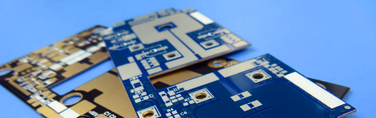
PCB Technology Is Facing New Challenges in 5G Era, What Should We Do?
PCB Technology Is Facing New Challenges in 5G Era, What Should We Do?
5G communication has more and more influence on people's life, and new mobile phones will step into the 5G era bit by bit. Today, let's take a look at what challenges 5G communication brings to PCB industry.
Material requirements: A very clear direction of 5G PCB is high frequency and high speed material and plate making. In terms of high frequency materials, it is obvious that leading materials manufacturers in the field of traditional high speed, such as Lianmao and Panasonic, have begun to lay out high frequency plates and launched a series of new materials. This will break the current situation of Rogers alone in the field of high-frequency sheet metal. After healthy competition, the performance, convenience and availability of materials will be greatly enhanced. Therefore, high-frequency materials localization is an inevitable trend.
Requirements for quality monitoring: Due to the improvement of 5G signal rate, plate making deviation has a greater impact on signal performance, which requires more stringent production deviation control of plate making. However, the existing mainstream plate making process and equipment are not updated much, which will become a bottleneck for future technological development. How PCB manufacturers break the situation is very important.
Requirements for manufacturing process: The enhancement of functions of 5G-related application products will increase the demand for high-density PCB, and HDI will also become an important technology area. Multi-stage HDI products and even arbitrary sequential interconnect products will be promoted, and new technologies such as buried resistance and buried capacity will be applied more and more.
The uniformity of copper thickness, precision of line width, alignment between layers, thickness of interlayer medium, control precision of back drilling depth and plasma drilling ability of PCB are all worthy of further study.
Requirements for PCB design: panel selection should meet the requirements of high frequency and high speed, impedance matching, cascade planning, wiring spacing/holes should meet the requirements of signal integrity, which can be started from six aspects: loss, embedding, high frequency phase/amplitude, mixed voltage, heat dissipation and PIM.
Requirements for equipment and instruments: high-precision equipment and pretreatment line with less coarsening of copper surface are ideal processing equipment at present; And the test equipment has no source intermodulation tester, flying needle impedance tester, loss test equipment.
Precision graphic transfer and vacuum etching equipment, real-time monitoring and feedback data changes in line width and coupling spacing detection equipment; Electroplating equipment with good uniformity and high-precision lamination equipment can also meet the production requirements of 5G PCB.
 6-11C Shidai Jingyuan, Fuyong, Baoan, Shenzhen, Guangdong, China 518103


For inquiries about our products or pricelist, please leave to us and we will be in touch within 24 hours.
© Copyright: 2026 Shenzhen Bicheng Electronics Technology Co., Ltd.. All Rights Reserved.

IPv6 network supported


