
 Call Us Now !
Tel : +86 755 27374946
Call Us Now !
Tel : +86 755 27374946
 Order Online Now !
Email : info@bichengpcb.com
Order Online Now !
Email : info@bichengpcb.com
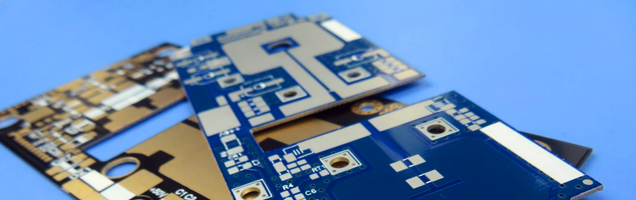
Technical Requirements for 5G Millimeter Wave HF PCB Copper-clad Board
Technical Requirements for 5G Millimeter Wave HF PCB Copper-clad Board
As the development of electronic communication products has experienced several stages, such as 1G, 2G, 3G and 4G, and is now entering the stage of the 5th generation of communication products. As the 5th generation of electronic communication, compared with 4G, 5G has undergone great changes in peak rate, spectral efficiency, delay and other aspects, which puts forward new requirements for high frequency board and copper-clad plate materials.
5G communication to PCB technology requirements
With the trend of miniaturization and increasing capacity of communication products, the design space of the front end of the product is severely squeezed. In order to relieve the design pressure, communication chip manufacturers have to choose to develop higher rate IC products to meet the demand of large capacity and small volume products. However, with the increase of speed, the pressure on signal integrity engineers is not alleviated but increased. High-speed products can be achieved by using less wiring, but the increase of speed directly leads to strict requirements on signal quality and less and less margin. Under 10Gbps signal, the UI of the signal can reach the bit width of 100ps, but under 25Gbps signal, the bit width of the signal is only 40ps, which means that optimization design should be carried out in every link of the channel to strive for the margin of every PS.
5G communication, as the fifth generation of mobile communication products, has applied many new technologies, but in any case, it cannot do without PCB as the carrier. The requirements for PCB are more and more stringent, especially for PCB substrate materials, processing technology, surface treatment and other very high requirements.
The increasing working frequency of 5G communication products has brought new requirements to the manufacturing process of printed boards. Millimeter-wave PCBS are usually multi-layer structures, and microstrip lines and grounded coplanar waveguide circuits are usually located in the outermost layer of the multi-layer structure. Millimeter wave belongs to the very high frequency (EHF) range in the whole microwave field. The higher the frequency is, the higher the dimensional accuracy of the circuit is required.
Comparison between 5G and 4G on PCB process capacity requirements
1. Appearance control requirements: The microstrip lines in key areas are not allowed to have pits and scratches, because the pcb stripline of high-frequency PCB transmit high-frequency electrical pulse signals instead of current. Pits, gaps, pinholes and other defects on high-frequency lines will affect transmission, and any such small defects are not allowed.
2. Control the corner of the microstrip antenna to improve the gain, direction and standing wave of the antenna; To avoid the resonance frequency deviation to high frequency and improve the margin of antenna design, it is necessary to control the Corner sharpness control (EA) of the microstrip antenna patch, such as ≤20um, 30um, etc. The antenna high frequency wholesale is what we can do for you.
3. For single-channel 112G high-speed products, PCB copper-clad board materials are required to have low Dk Df, new resin, glass cloth and copper foil technologies are required, and PCB process back drilling precision is required to be higher, thickness tolerance control is more strict, aperture smaller, etc.
4. HDI high-density technology application: PCB technology requirements of PRODUCTS in 5G era, including second-order HDI technology application, multiple lamination technology, asymmetric design, 0.15mm micro-hole, 0.20mm high-density hole wall spacing, mixing of materials of different systems, etc.
5G communication PCB technical difficulties
5G chips require smaller PCB hole spacing, with the maximum hole wall spacing of 0.20mm and the minimum aperture of 0.15mm. Such high-density layout brings great challenges to CCL materials and PCB processing technology, such as CAF problems and cracks between heated holes. The maximum aspect ratio is more than 20:1. How to prevent the problem of broken needle during drilling, how to improve the aspect ratio ability of PCB electroplating, and how to prevent the problem of copper free hole wall are the urgent problems of PCB technology.
5G communication products require higher frequency and speed, and high-speed and high-frequency signals pay attention to the consistency of transmission line loss and impedance timely delay. For PCB substrate materials, smaller Dk/Df is required, and the higher Df is, the more obvious lag effect is. The research focus of PCB coppers in the industry mainly focuses on Low Dk/Df. The development of Low CTE and high thermal conductivity materials requires supporting copper foil, glass cloth, resin, filler and other upstream and downstream supply chains.
Lower loss copper clad plate material requirements
In the next 3-5 years, 5G communication of the Internet of Everything will be mass-produced, and 6G of the Internet of Heaven and Earth will start pre-research, which will require high-speed copper clad panel technology to develop in the direction of lower loss Df, lower dielectric constant Dk, higher reliability and lower CTE technology. Accordingly, copper clad plate mainly composed of copper foil, resin, glass cloth, filler and so on should also be synchronized to the direction of development.
Low loss resin material
In order to meet the requirements of 5G high-speed products, the traditional FR4 epoxy resin system can not meet the requirements, requiring the copper clad resin Dk/Df smaller, the resin system is gradually closer to the mixed resin or PTFE material.
The PCB thickness of high-speed and high-frequency products of 5G communication is getting higher and higher, the aperture is getting smaller and smaller, and the ASPECT ratio of PCB will be larger. This requires the copper clad resin to have lower loss. At the same time of loss reduction, defects such as hole wall separation or hole wall fracture cannot occur.
In the design of microstrip line or ribbon line, when the high frequency signal is transmitted in the wire, most of the electromagnetic wave energy will be bound in the medium layer between the wire and the shielding layer (ground), and the skin effect will cause the transmission of high frequency signal to gather in the thin layer of the wire surface, and the closer to the wire surface, the higher the alternating current density. For the microstrip line, the skin effect will appear at the position where the microstrip line contacts the medium. The smaller the copper foil roughness, the smaller the dielectric loss, HVLP copper foil dielectric loss is significantly less than RTF copper foil, from the product performance of 5G, the need for lower roughness HVLP copper foil, but the lower the copper foil roughness, peel strength is also smaller, there will be thin line or small pad peel risk.
Glass cloth technology with low loss and low expansion rate
In order to meet the requirements of high-speed PCB design of 5G communication products and 100x100mm large-size chip application, the Dk/Df and CTE of high-speed copper clad glass cloth should be smaller. If the MATERIAL CTE is too large, welding spot cracking and other defects will occur in PCBA assembly welding. In order to develop high-speed copper clad plate with Low CTE, the CTE of glass cloth is required to be ≦3.0 PPM /℃, etc. In order to meet the requirements of CTE, it is necessary to innovate the glass fiber raw material formula and drawing technology, and prepare glass cloth with lower CTE to meet the requirements of 5G or 6G communication technology.
Stability of medium thickness
The uniformity and fluctuation of the structure, composition and thickness of the dielectric layer affect the characteristic impedance values. Under the same thickness of the dielectric layer, the characteristic impedance values of the dielectric layer composed of 106, 1080, 2116 and 1035 resin are different. Therefore, it can be understood that the characteristic impedance values are not the same everywhere in the PCB dielectric layer. Therefore, in high frequency and high speed digital signal transmission 5G high frequency circuit board, it is advisable to choose thin glass fiber cloth or open fiber flat cloth to reduce the fluctuation of characteristic impedance value. The Dk value of materials between batches must be controlled within a certain range, and the thickness uniformity of the medium layer should be good. Make sure Dk changes within 0.5.
 6-11C Shidai Jingyuan, Fuyong, Baoan, Shenzhen, Guangdong, China 518103


For inquiries about our products or pricelist, please leave to us and we will be in touch within 24 hours.
© Copyright: 2026 Shenzhen Bicheng Electronics Technology Co., Ltd.. All Rights Reserved.

IPv6 network supported


