
 Call Us Now !
Tel : +86 755 27374946
Call Us Now !
Tel : +86 755 27374946
 Order Online Now !
Email : info@bichengpcb.com
Order Online Now !
Email : info@bichengpcb.com
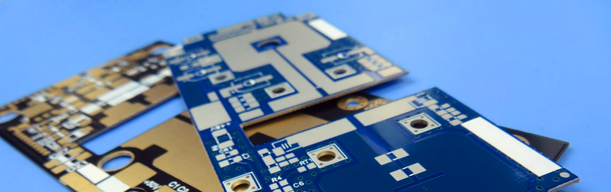
Top 10 Unacceptable Quality Problems of Printed Circuit Board
There are many control points in the whole production process, the board will be broken if there is a little bit of carelessness, the quality problems of PCB are emerging endlessly, this is also a headache to people, because if only one piece has a problem, then most of the devices will also cannot be used.
In addition to the above problems, there are also some problems with high potential risks, we have compiled a total of top ten problems, listed here and with some handling experience to share with you
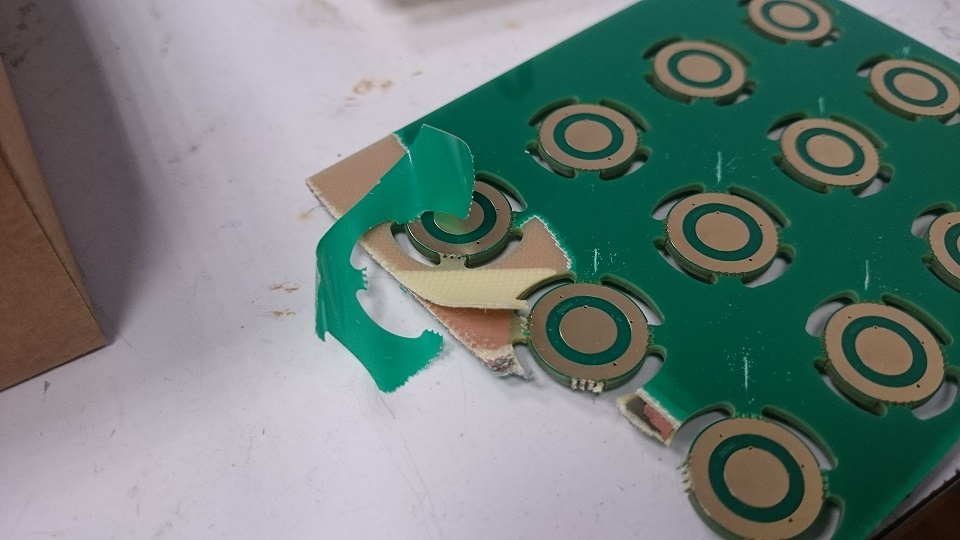
1.【Delamination】
Delamination is a long-standing problem of PCB, steadily ranking the first of the common problems. The causes may be as follows:
(1) It is improperly packaged or stored, or affected with damp;
(2) Too long time of storage, which exceeds the storage period, PCB board is affected with damp;
(3) The supplier’s material or process problems;
(4) Poor material selection of design and poor distribution of copper surface.
The problem of being affected with damp is easy to happen, Even if you choose a good package, and there is a constant temperature and humidity warehouse, but the transportation and temporary storage process cannot be controlled. But being affected with damp can still be solved, vacuum conductive bags or aluminum foil bags can be a good protection against moisture intrusion, at the same time, it is required to put a humidity indicating card in the packaging bags. If the humidity indicating card is found to exceed the standard before use, it can be solved by baking before putting online, the baking condition is usually 120 degrees, 4H.
Common possible causes may include: poor black oxidation, PP or inner board is affected with damp, insufficient PP glue quantity, abnormal pressing, etc.. In order to reduce this kind of problems, special attention should be paid to the management of PCB suppliers to the corresponding processes and reliability tests of delamination. Taking the thermal stress test in the reliability test as an example, the requirement of pass standard of a good factory is no delamination of over 5 times, and confirmation will be conducted in each period of the sample stage and the mass production. However, the pass standard of ordinary factory may only twice, and confirm only once every several months. The simulation mounting IR test can also prevent more outgoing of defective products, which is an essential for an excellent PCB factory.
Of course, the PCB design of the design company itself can also bring hidden dangers of delamination. For example, there is often no requirement of the choice of plate Tg, the temperature resistance of ordinary Tg material will be relatively poor. In the era of lead-free becoming a mainstream, the selection of Tg above 145°C is relatively safe. In addition, the open large copper surface and too dense buried via area is also the hidden dangers of PCB separated layer, which need to be avoided in the design.
2.【Poor solderability】
Solderability is also one of the serious problems, especially batch problems. Its possible causes are board pollution, oxidation, black nickel, abnormal nickel thickness, solder mask SCUM (shadow), too long time of storage, moisture absorption, solder mask with PAD, too thick (repair).
Contamination and moisture absorption problems are relatively easier to be solved, other problems are more troublesome, and these problems cannot be found through incoming quality inspection, at this time, you need to focus on the process capability and quality control plan of PCB factory. Take black nickel for example, you need check if the PCB factory send chemical gold (chemical gold) out, whether their analysis frequency medicinal liquid of chemical gold line is adequate, whether the concentration is stable, whether regular gold stripping test and phosphorus content test are set for detection, whether the internal solderability test are well executed etc.. If all of these can be well solved, then there will be little possibility of batch problem. While for solder mask PAD and poor repair, you need to understand PCB suppliers’ standards for maintenance, whether the inspectors and maintenance personnel have a good appraisal appointment system, at the same time, you shall clearly define that the pad-intensive areas cannot be repaired (such as BGA and QFP).
3.【Board bending and warpage】
The reasons that may cause board bending and warpage are: the problem of supplier’s selection of material, abnormal production process, poor control of rework, improper transportation or storage, design of broken hole is not strong enough, the copper area difference of each layer is too large, etc.. The last two design issues need to be conducted with design review in earlier stage for avoidance, at the same time, you can require PCB factory to simulate mounting IR condition for test, in order to avoid board bending after the furnace. For some thin plates, you can require to press wood-pulp board up and down when packing and after which to conduct package, to avoid subsequent deformation, add a fixture while mounting to prevent excessive weight of device from bending the board.
4.【Scratch, copper exposure】
Scratch and copper exposure are the defects that most test the management system and execution of PCB factory. This problem is either serious or nothing serious, but it does bring quality concerns. Many PCB companies will say that this problem is difficult to improve. In many cases, it is not difficult to change it, but whether to change it or not, whether you have incentive to change it. All DPPMs delivered by the PCB factory who has promoted the project carefully have made significant improvements. Therefore, the solution trick of this problem lies in: push, pressure.
5.【Poor impedance control】
PCB impedance is an important indicator related to radio frequency performance of the mobile phone board, the common problem is the larger impedance differences between PCB batches. Since the impedance test strips are usually made on the large board side of the PCB and cannot be shipped with the boards, so the supplier can be required to attach the impedance strips and the test reports of that batch for reference at each time of shipping, at the same time, the comparison data of board edge diameter and board interior wire diameter are required to be provided.
6.【BGA soldering tin void】
BGA soldering tin void can lead to poor function of the master chip and may not be detected during testing, with a high risk of hiding. So now many SMT factories pass X-RAY for inspection after mounting. The possible reasons of this type of defect can be residual liquid or impurities in the PCB hole, vapors after high temperature, or poor hole pattern on the BGA pad. So nowadays many HDI boards require plating pore-filling or semi-pore-filling to avoid this problem.
7.【Solder mask foaming/dropping】
Such problems are usually abnormalities of process control of PCB solder mask, or the used solder mask ink is not suitable (bargains, non chemical gold ink, improper mounting flux), it also could be too high temperature of mounting and rework. To prevent batch problems, PCB suppliers need to develop the corresponding reliability testing requirements, to control in different stages.
8.【Poor via plug】
Poor via plug is mainly the lack of technical capacity of PCB factory or caused by the simplifying the process, its performance is that the via plug is not full, there is copper exposure or pseudo-exposed copper in hole ring, which may cause the problems of insufficient quantity of soldering tin, short circuit with patch or assembled device, residual impurities in the hole and so on. This problem can be found in visual inspection, so it can be controlled in incoming quality inspection, requiring PCB factory to improve.
9.【Poor size】
There are many possible reasons for poor size, it is easy to cause harmomegathus on PCB production process, the supplier adjusted the drilling program / graphics ratio / forming CNC program, which may cause misplaced mounting, poor match of the structural parts and other issues. As such problems are very difficult to be detected and which can only depend on good process control of the supplier, so special attention shall be paid to selection of suppliers.
Galvanic effect is the primary cell reaction learned in high school chemistry, which appears in the OSP process of selective chemical gold plate. Due to the potential difference between gold and copper, the copper pad connected to the large gold surface in the OSP treatment process will continuously lose electrons and dissolve into divalent copper ions, resulting in the pad becoming smaller, affecting the mounting of subsequent components and reliability.
Although this problem does not often happen, while it will be batch problem once occurs. The board factory with experience of manufacturing mobile phone PCB will screen out this part of pad through computer software, to pre-compensate it before the design, and set special rework conditions and limit the number of reworks to avoid occurrence of problems. So this problem can be confirmed in advance when reviewing the board factory.
 6-11C Shidai Jingyuan, Fuyong, Baoan, Shenzhen, Guangdong, China 518103


For inquiries about our products or pricelist, please leave to us and we will be in touch within 24 hours.
© Copyright: 2026 Shenzhen Bicheng Electronics Technology Co., Ltd.. All Rights Reserved.

IPv6 network supported


