The Technical Development of PCB Circuit Board
In recent years, the focus of the printed circuit board market has shifted from computers to communications, and in the past two years, it has shifted to mobile terminals such as smartphones and tablet computers. Therefore,
HDI boards for mobile terminals are the main point of PCB growth. Mobile terminals represented by smart phones drive HDI boards to be higher density and thinner. PCBs are all developing towards high-density thin lines, especially HDI boards. In the past, the definition of HDI board was that the line width/line spacing was 0.1 mm/0.1 mm and below, but now the industry basically achieves 60µm, and the advanced one is 40µm. PCB circuit pattern formation, traditionally is a chemical etching process (subtraction method) after photoimaging on a copper foil substrate. This method has many processes, difficult to control and high cost. The current fine circuit fabrication tends to be semi-additive or improved semi-fabrication. The bonding force between the conductor and the insulating substrate, the customary practice is to increase the surface roughness to increase the surface area and improve the bonding force, such as strengthening the decontamination treatment to roughen the surface of the resin layer, and use high-profile copper foil or oxidation to treat the copper surface. For thin wires, this physical method is not enough to ensure the bonding force. Therefore, the electroless copper-plated high-adhesion copper foil on the smooth resin surface was developed. For example, "molecular bonding technology" is to chemically treat the surface of the resin substrate to form a functional group that can be closely combined with the copper layer. In addition, there is the transfer of dry film imaging patterns during the production of fine lines, and the surface treatment of copper foil is one of the key factors for success. Use the best combination of surface cleaners and microetchants to provide a clean surface with sufficient area to promote dry film adhesion. Use chemical cleaning to remove the anti-discoloration treatment layer on the surface of the copper foil, as well as to remove dirt and oxides. Select an appropriate chemical cleaner according to the type of copper foil, by micro-etching the surface of the copper foil. In order to combine the imaging dry film with the copper layer, the solder mask pattern and the thin circuit reliably, the method of non-physical roughening of the surface should also be adopted.
Semi-Additive Laminated Substrates
At present, the hot spot of the semi-additive method is to use insulating dielectric film laminates. SAP is more advantageous than MSAP in terms of fine circuit realization and production cost. The thermal curing resin for SAP lamination is formed by electroplating copper after laser drilling to form via holes and circuit patterns. At present, the international HDI laminate materials use epoxy resin with different curing agents to add inorganic powder to improve the rigidity of the material and reduce the CTE, and also use glass fiber cloth to enhance the rigidity.
Copper plated hole filling
From the point of view of reliability, the interconnection holes adopt the electroplating copper hole filling technology, including blind hole copper filling and through hole copper filling. The ability of copper plating to fill holes is manifested in filling: whether there are voids in the holes closed by copper; flatness: the degree of dimple in the copper-plated holes; aspect ratio: the thickness of the plate (hole depth) and the diameter of the hole. Proportion.
Flip chip package IC package carrier board technology
Organic substrates account for more than one-third of the market share in global semiconductor packaging. FC-CSP and FC-PBGA surged as production of mobile phones and tablets grew. The package carrier is replaced by an organic substrate, and the pitch of the package carrier is getting smaller and smaller, and the typical line width/line spacing is now 15µm. future development trends. In BGA and CSP fine-pitch carriers will continue, while coreless boards and four or more layers of carrier boards are more used, the roadmap shows that the feature size of the carrier board is smaller, and the performance focus requires low dielectric, low Coefficient of thermal expansion and high heat resistance, pursuing low-cost substrates while meeting performance targets.
Meet the needs of high frequency and high speed PCB
Electronic communication technology from wired to wireless, from low frequency, low speed to high frequency, high speed. The current mobile phone performance has entered 4G and will move towards 5G, which means faster transmission speed and larger transmission capacity. The advent of the global cloud computing era has doubled the data traffic, and the high frequency and high speed of communication equipment is an inevitable trend. In order to meet the needs of high-frequency and high-speed transmission, in addition to reducing signal interference and loss in circuit design, maintaining signal integrity, and maintaining PCB manufacturing to meet design requirements, it is important to have high-performance substrates. To address PCB increase speed and signal integrity, the main focus is on electrical signal loss properties. The key factors of substrate selection are dielectric constant (Dk) and dielectric loss (Df). When Dk is lower than 4 and Df is less than 0.010, it is a medium Dk/Df laminate, and when Dk is lower than 3.7 and Df is less than 0.005, it is low Dk/ Df grade laminate. The surface roughness (profile) of conductor copper in high-speed PCBs is also an important factor affecting signal transmission loss, especially for signals in the range above 10 GHz. Copper foil roughness needs to be less than 1µm at 10 GHz, and it is better to use ultra-planar copper foil (surface roughness 0.04µm).
Improve heat and heat dissipation
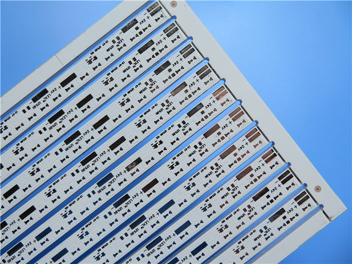
With the miniaturization and high function of electronic equipment, which generates high heat generation, the thermal management requirements of electronic equipment continue to increase. One solution chosen is to develop thermally conductive printed circuit boards. PCBs are required to have high thermal conductivity and heat resistance, and efforts have been made for the past ten years. Existing high heat dissipation PCBs such as planar thick copper substrate PCB, aluminum metal base PCB, aluminum metal core double-sided PCB, copper base flat PCB, aluminum base cavity PCB, embedded metal block PCB, bendable aluminum base PCB, etc. . The metal substrate (IMS) or metal core printed circuit board is used to dissipate heat from the heat-generating components, reducing the volume and cost compared to traditional radiators and fans. At present, most metal substrates or metal cores are metal aluminum. The advantages of aluminum substrates are simple and economical, reliable electronic connection, high thermal conductivity and strength, no soldering, lead-free environmental protection, etc., and can be designed and applied from consumer goods to automobiles, military products and aerospace.

New trends in flexible and rigid-flex board technology
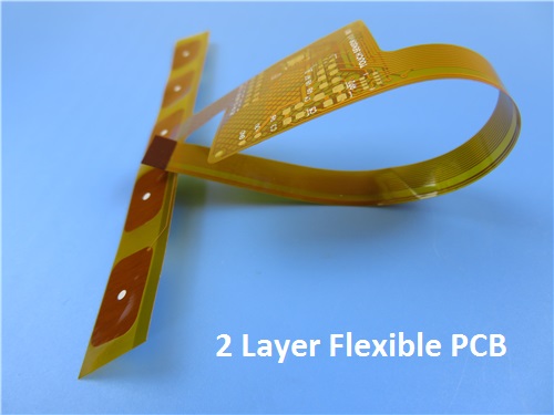
The miniaturization and thinning of electronic equipment will inevitably use a large number of flexible printed circuit boards and rigid-flex printed circuit boards (R-FPCB). With the expansion of the application area, there will be many new performance requirements in addition to the increase in number. Polyimide film is available in colorless and transparent, white, black and yellow, with high heat resistance and low CTE properties, suitable for different occasions. There is also a market for cost-effective polyester film substrates, with new performance challenges such as high elasticity, dimensional stability, film surface quality, and film opto-coupling and environmental resistance to meet changing end-user requirements. Like rigid HDI boards, FPCBs must meet the requirements of high-speed and high-frequency signal transmission. The dielectric constant and dielectric loss of flexible substrates must be paid attention to. Flexible circuits can be constructed using polytetrafluoroethylene and advanced polyimide substrates. . Adding inorganic powders and carbon fiber fillers to polyimide resins produces a flexible thermally conductive substrate with a three-layer structure. Selected inorganic fillers are aluminum nitride (AlN), aluminum oxide (Al 2O3) and hexagonal boron nitride (HBN).

In terms of
FPCB manufacturing technology, direct metallization on polyimide (PI) film to manufacture
double-sided FPCB technology has been developing. There is a new technology of molecular bonding agent aqueous solution, which does not change the surface roughness of PI film and can increase chemical deposition. Copper layer bond strength. The PI film is used for molecular bonding treatment and then chemically copper is directly plated, and the double-sided flexible printed circuit board is produced through the semi-additive process, which simplifies the process and is environmentally friendly, and meets the requirements for bonding force, flexibility and reliability. There is also a printing autocatalytic electronic circuit technology, which is produced in rolls (R2R), firstly printing and coating the autocatalytic ink on the PET film, and then entering the electroless copper plating tank, because the ink has autocatalytic ability on the ink. A copper layer is deposited to form a copper conductor pattern, and the metal thin circuit on the PET film is completed. For example, ultra-thin flexible
multi-layer boards, four-layer FPCBs are thinned from conventional 0.4 mm to about 0.2 mm; high-speed transmission flexible boards use low Dk and low Df polyimide substrates to meet 5Gbps transmission speed requirements; large Power flexible board, using conductors thicker than 100µm to meet the needs of high-power and high-current circuits; high heat dissipation metal-based flexible board is an R-FPCB partially using metal plate substrate; tactile-sensitive flexible board, by pressure sensing The membrane and the electrode are sandwiched between two polyimide films to form a flexible tactile sensor; a stretchable flexible board or a
rigid-flex board, the flexible substrate is an elastomer, and the shape of the metal wire pattern is improved to become stretchable .
Printed electronics
The history of printed electronics is very early, but it has only flourished in recent years. Printed electronics technology is used in the printed circuit industry and is a part of printed circuit technology. The continuous development of printed electronics can see that the prospects for commercial applications are very broad. Now PCB manufacturers have invested in printed electronics. They started with flexible boards and replaced printed circuit boards (PCBs) with printed electronic circuits (PEC). Printed electronics technology is closest to FPCB. Currently, there are many substrates and ink materials. Once there is a breakthrough in performance and cost, it will be widely used, and cost reduction will open up a larger market. Hybrid systems of organic and printed electronics contribute to the growth of the industry. A hybrid system combining traditional silicon and printed electronic components, this could open up new PCB industries. These hybrid technologies include large area lithography, screen printing or inkjet printing, and flexible PCB technologies. An important aspect of printed electronics is materials, including substrates and functional inks. In addition to the existing FPCB application, flexible substrates have also developed higher-performance substrates. Currently, there are high-dielectric substrate materials composed of ceramics and polymer resins, as well as high-temperature substrates, low-temperature substrates and colorless transparent substrates. , yellow substrate, etc. In addition to using some polymer materials, printed electronics also need functional ink materials, mainly conductive inks, which are constantly developing towards improving conductivity, printing adaptability, and low cost. Currently, conductive inks can be selected for printed electronic products. There are many kinds. There are also piezoelectric, pyroelectric, and ferroelectric materials, which can be used in combination in printed electronics to provide versatility.
Another important aspect of printed electronics technology is the printing process and corresponding printing equipment, which is an innovative development of traditional printing technology. Printed electronics can apply different printing methods such as gravure printing, letterpress printing, screen printing and inkjet printing. Screen printing has been applied in PCB manufacturing, with mature technology and low cost. Currently, it is developing towards automation and high precision. The application range of inkjet printing in PCB manufacturing is expanding, from marking symbols, solder resists to resist patterns, and further direct printing of conductive graphics; at the same time, inkjet printing is developing towards high-definition and rapid graphics. Such as the new aerosol jet technology is obviously superior to piezoelectric jet printing, the formation of wires meets the requirements of fineness and three-dimensionality, and electronic circuits and components can be directly printed on flat or three-dimensional components. There is also an inkjet printing method that uses laser irradiation to instantly cure the ink. The ratio of the thickness to the width of the conductive line is more than 1.0. For example, the line width is 10µm, and the line height is also 10µm. An example is the production of a PI film. FPCB with a line width of 30µm and a line thickness of 20µm .
Embedded Component Printed Circuit Technology
Embedded component printed circuit board (EDPCB) is a product that realizes high-density electronic interconnection, and embedded component technology has great potential in PCB. The embedded component PCB manufacturing technology has improved the function and value of the PCB. In addition to the application in communication products, it also provides opportunities in the fields of automotive, medical and industrial applications. The development of EDPCB, from the printed resistors made of carbon paste and the thin film resistors made of nickel-phosphorus alloy foils, and the planar capacitors formed by sandwiching high dielectric constant substrates, to form embedded passive component printed boards, to embedded ICs Chips, embedded patch components, and embedded active and passive components printed boards. The issues facing now include the complexity of embedded components and the thinning of EDPCB, as well as heat dissipation and thermal deformation control, and final inspection technology.
Surface Finishing Technology
The copper layer on the surface of the PCB needs to be protected to prevent oxidation and deterioration of the copper and to provide a reliable surface for connections during assembly. Some commonly used surface finishes in PCB manufacturing include lead-containing or lead-free hot air leveling solder, immersion tin, organic solderability protective film, electroless nickel/gold plating, electroplating nickel/gold, etc. The surface finish of HDI board and IC package carrier board is now developed from electroless nickel/gold (ENIG) to electroless nickel/palladium/gold (ENEPIG), which is beneficial to prevent black disks from appearing after component installation and affect reliability. The palladium layer in the ENEPIG coating has been analyzed at present. The palladium layer structure includes pure palladium and palladium-phosphorus alloy. They have different hardnesses. Therefore, different palladium layers should be selected for wire bonding and welding. After the reliability impact assessment, the presence of trace amounts of palladium will increase the growth thickness of copper and tin; while too much palladium content will produce brittle palladium-tin alloys, which will reduce the strength of solder joints, so an appropriate thickness of palladium is required. From the point of view of PCB fine lines, electroless palladium/immersion gold (EPIG) surface treatment is better than electroless nickel/palladium/immersion gold (ENEPIG), reducing the impact on fine pattern line width/line spacing. The EPIG coating is thinner and will not cause circuit deformation; EPIG can meet the requirements after soldering test and wire bonding test. There are new direct electroless palladium (EP) or direct immersion gold (DIG) coatings on copper, or electroless palladium and autocatalytic gold (EPAG) coatings on copper, which have the advantage of being suitable for press bonding of gold or copper wires. Better high frequency characteristics due to no nickel layer, thin coating more suitable for fine line patterns, and reduced process and cost. The improvement of the final finishing layer of PCB, and the introduction of electroless nickel immersion silver (NiAg) coating, silver has good electrical conductivity, solderability, nickel has corrosion resistance. Organic coating OSP for performance improvement, improve heat resistance and solderability. There is also an organic-to-metal composite (OM) coating, which has a good price/performance ratio for coating the copper surface of PCB with OM coating.
Clean manufacturing
"Green" and "environmentally friendly" are now important signs of the advancement of PCB manufacturing technology. In addition to trying to adopt revolutionary cleaner production technologies such as printed electronics and 3D printing, the improvement of existing PCB manufacturing technologies towards cleaner production is ongoing. Such as finding materials to replace toxic and hazardous substances, reducing processing steps, and reducing the consumption of chemicals, as well as reducing the amount of water and energy, and recyclable materials. Specifically, there are halogen-free substrates that use non-toxic inorganic materials as flame retardants, and also improve electrical properties, thermal conductivity and thermal expansion coefficient; use laser direct imaging to reduce operating procedures and material consumption; use semi-additive methods to reduce electroplating copper and Etching copper consumption; using direct metallization hole process, and eliminating toxic and harmful substances in chemical copper precipitation solution; using conductive paste printing to make via hole interconnection processing clean and easy. Direct metallization technology has existed for a long time and has matured over the years. The direct metallization process has carbon black system and conductive polymer system, replaces palladium activation with carbon or graphite, conductive polymer, and removes toxic formaldehyde, cyanide and intractable EDTA complexing agent in the electroless copper precipitation liquid. Introduced colloidal graphite direct hole metallization technology with stable dispersion and good adsorption with various resins. The colloidal graphite direct metallization process has been used in rigid PCB manufacturing for many years, and can now be applied to HDI boards, flexible boards and rigid-flex boards with complex blind vias, buried vias and any layer interconnection, which can reduce the number of processes and equipment sites, waste water It is beneficial to environmental protection, and improves production efficiency and high reliability of the final product. What was once called waste or even hazardous waste in the PCB production process is no longer "waste". For example, excess copper etching solution, micro-etching treatment solution, and electroplating cleaning solution tend to be recycled online. Some newly designed production line equipment, whether it is an etching line or a vertical electroplating line and a horizontal electroplating line, have considered the configuration of online recycling and regeneration devices, as well as reasonable configuration of air knives between sections, energy saving of circulating pumps, automatic analysis of adding liquid medicine to prolong Measures such as the life of the liquid medicine are not only conducive to improving the quality, but also conducive to energy saving and environmental protection.

 Call Us Now !
Tel : +86 755 27374946
 Order Online Now !
Email : info@bichengpcb.com


