
 Call Us Now !
Tel : +86 755 27374946
Call Us Now !
Tel : +86 755 27374946
 Order Online Now !
Email : info@bichengpcb.com
Order Online Now !
Email : info@bichengpcb.com
Multilayer Stackup Design: Minimizing Crosstalk in High-Speed PCBs
Multilayer Stackup Design: Minimizing Crosstalk in High-Speed PCBs
Introduction
In high-speed PCB design, signal integrity is paramount. As data rates increase, crosstalk—unwanted electromagnetic coupling between traces—becomes a critical challenge. A well-optimized multilayer stackup is essential to minimize crosstalk while ensuring signal integrity, power delivery, and manufacturability.
This article explores how to design a 6-layer PCB stackup for high-speed applications, using our RO4350B + S1000-2M construction as a case study. We’ll examine material selection, layer arrangement, impedance control, and design techniques to reduce crosstalk.
Understanding Crosstalk in High-Speed PCBs
Crosstalk occurs when signals on adjacent traces interfere due to capacitive (electric field) and inductive (magnetic field) coupling. Key factors influencing crosstalk include:
A well-designed 6-layer hybrid PCB stackup can mitigate these issues by providing:
✔Shielded signal layers
✔Controlled impedance routing
✔Optimized dielectric spacing
Case Study: 6-Layer High-Speed PCB Stackup
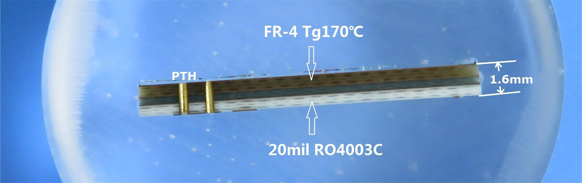
Our 6-layer PCB (76.5mm x 83mm) is designed for high-speed applications with RO4350B microwave laminate and S1000-2M high-Tg FR4.
PCB Stackup Breakdown
|
Layer |
Material |
Thickness |
Function |
|
L1 |
Copper (35μm) |
- |
Signal (Top Layer, 50Ω impedance) |
|
PP1 |
RO4350B |
0.254mm |
Low-loss dielectric |
|
L2 |
Copper (35μm) |
- |
Ground Plane |
|
PP2 |
Prepreg (1080) |
0.127mm |
Bonding layer |
|
L3 |
Copper (35μm) |
- |
Signal (Internal High-Speed) |
|
Core |
S1000-2M |
0.254mm |
High-Tg FR4 for stability |
|
L4 |
Copper (35μm) |
- |
Power Plane |
|
PP3 |
Prepreg (1080) |
0.127mm |
Bonding layer |
|
L5 |
Copper (35μm) |
- |
Signal (Internal High-Speed) |
|
PP4 |
RO4350B |
0.254mm |
Low-loss dielectric |
|
L6 |
Copper (35μm) |
- |
Signal (Bottom Layer, 50Ω impedance) |

Key Features for Crosstalk Reduction
1. Rogers RO4350B for Critical Signal Layers
2. ShengyiS1000-2M Core for Mechanical Stability
3.Impedance Control (50Ωon Top Layer)
4.Shielding with Ground & Power Planes
5.Blind Vias (L1-L2) for Signal Integrity
Design Techniques to Minimize Crosstalk
1. 3W Rule for Trace Spacing
Keep spacing≥3x trace width (e.g., 12mil spacing for 4mil traces).
2. Differential Pair Routing
Maintain consistent spacing & length matching to reduce EMI.
3. Avoid Parallel Routing on Adjacent Layers
Orthogonal routing (90°angles) reduces capacitive coupling.
4. Use Ground-Filled Areas Between Signals
Additional copper pours act as shields.
5. Controlled Dielectric Thickness
Thinner prepreg (0.127mm) reduces crosstalk between layers.
Why This Stackup Works for High-Speed Designs?
✅Low-Loss Materials (RO4350B)→Better signal integrity at GHz frequencies.
✅Solid Ground/Power Planes→Shields high-speed signals.
✅Blind Vias & Impedance Control→Minimizes reflections & EMI.
✅Thermally Stable Core (S1000-2M)→Ensures reliability in harsh conditions.
Applications of This PCB Design
Conclusion
A well-optimized multilayer stackup is critical for minimizing crosstalk inhigh-speed PCBs. By using low-loss materials (RO4350B), proper shielding, and controlled impedance routing, this 6-layer hybrid circuit board design ensures signal integrity while meeting IPC-Class-2 standards.
For high-frequency, high-speed, or RF applications, our RO4350B + S1000-2M stackup provides an ideal balance of performance, reliability, and cost-effectiveness.
Need a custom high-speed PCB solution? Contact us today for expert design and manufacturing support!
Categories
New Blog
Tags
 6-11C Shidai Jingyuan, Fuyong, Baoan, Shenzhen, Guangdong, China 518103


For inquiries about our products or pricelist, please leave to us and we will be in touch within 24 hours.
© Copyright: 2026 Shenzhen Bicheng Electronics Technology Co., Ltd.. All Rights Reserved.

IPv6 network supported


