
 Call Us Now !
Tel : +86 755 27374946
Call Us Now !
Tel : +86 755 27374946
 Order Online Now !
Email : info@bichengpcb.com
Order Online Now !
Email : info@bichengpcb.com
What Are the Design Considerations for Hybrid High-Frequency PCBs?
What Are the Design Considerations for Hybrid High-Frequency PCBs?
Introduction
Hybrid (mixed dielectric) high-frequency PCBs combine different materials to optimize electrical performance, thermal stability, and manufacturability. These mixed dielectric hybrid boards are widely used in RF/microwave applications, aerospace, radar systems, and telecommunications, where signal integrity and thermal management are critical.
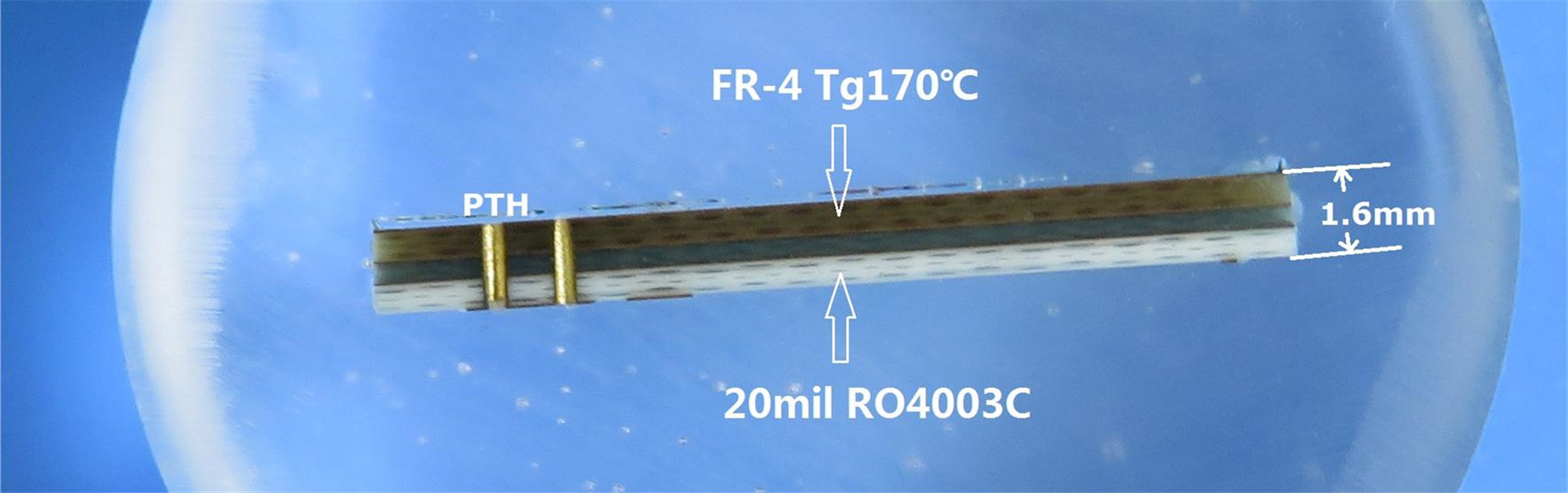
Designing hybrid PCB requires careful consideration of material properties, layer stackup, signal integrity, and manufacturing constraints. In this article, we explore key design considerations and provide practical insights, using a 4-layer hybrid PCB (RO4350B + High-Tg FR-4 S1000-2M) as an example.
1. Material Selection and Compatibility
Key Factors in Material Selection
Dielectric Constant (Dk) & Loss Tangent (Df):
Thermal Expansion (CTE) Mismatch:
Thermal Conductivity & Tg:

Example PCB Construction
Our 4-layer hybrid circuit board combines:
Signal Layers (RO4350B): Optimized for RF performance.
Core/Prepreg (FR-4 S1000-2M): Provides structural integrity.
Stackup:
Layer 1 (RF Signal): 35μm Cu + RO4350B (0.254mm)
Layer 2 (Ground/Power): 35μm Cu + Prepreg (0.254mm)
Layer 3 (Inner Signal): 35μm Cu + S1000-2M (0.8mm)
Layer 4 (Bottom Layer): 35μm Cu
2. Signal Integrity and Impedance Control
Critical Design Rules
Controlled Impedance Routing:
Minimizing Crosstalk & Loss:
Via Optimization:
3.Thermal Management Considerations
Preventing Delamination & Warpage
Heat Dissipation Strategies
4. Manufacturing and Reliability
Fabrication Tolerances
Quality Assurance
5. Applications of Hybrid High-Frequency PCBs
Our example PCB (RO4350B + S1000-2M) is ideal for:
✅Radar & Guidance Systems (stable Dk, low loss)
✅5G & Millimeter-Wave Antennas (precise impedance control)
✅Aerospace & Defense Electronics (high thermal reliability)
Conclusion
Designing hybrid high-frequency PCBs requires a balance between material properties, signal integrity, and manufacturability. By selecting compatible materials (like RO4350B FR-4 hybrid PCB), optimizing stackup, and following best practices in impedance control and thermal management, engineers can achieve high-performance RF/microwave designs.
Looking for a reliable hybrid PCB supplier? Our 4-layer mixed-dielectric PCB (RO4350B + S1000-2M) meets stringent RF and thermal requirements while ensuring cost-effective production. Contact us today for your high-frequency PCB needs!
Categories
New Blog
Tags
 6-11C Shidai Jingyuan, Fuyong, Baoan, Shenzhen, Guangdong, China 518103


For inquiries about our products or pricelist, please leave to us and we will be in touch within 24 hours.
© Copyright: 2026 Shenzhen Bicheng Electronics Technology Co., Ltd.. All Rights Reserved.

IPv6 network supported


