
 Call Us Now !
Tel : +86 755 27374946
Call Us Now !
Tel : +86 755 27374946
 Order Online Now !
Email : info@bichengpcb.com
Order Online Now !
Email : info@bichengpcb.com
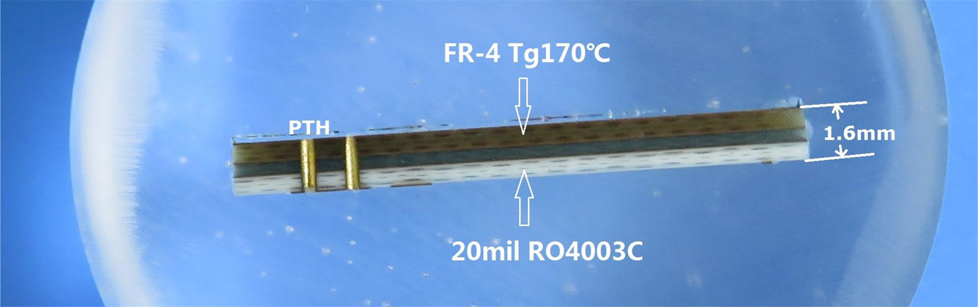
PTFE Materials Are Difficult to Process—How to Solve Lamination and Drilling Challenges?
PTFE Materials Are Difficult to Process—How to Solve Lamination and Drilling Challenges?
Introduction
Polytetrafluoroethylene (PTFE), commonly known by the brand name Teflon (TFE), is a high-performance material widely used in printed circuit boards (PCBs) for high-frequency applications. Its low dielectric constant (Dk) and dissipation factor (Df) make it ideal for RF, microwave, and millimeter-wave circuits. However, TFE materials like Rogers RT/duroid 5880 present significant challenges in lamination and drilling due to their unique properties.
In this article, we’ll explore the key difficulties in TFE material PCB fabrication and provide practical solutions to overcome them. We’ll also highlight how our 3-layer rigid PCB with RTduroid 5880 and RO4450F bonding ply successfully addresses these challenges while maintaining high-frequency performance.
Why TFE Materials Are Difficult to Process
PTFE-based laminates like RT/duroid 5880 offer outstanding electrical properties, including:
However, these benefits come with manufacturing challenges:
1. Lamination Difficulties
2. Drilling Challenges

Solutions for Successful TFE PCB Fabrication
1. Optimizing Lamination for TFE Materials
a) Use Special Bonding Materials
To improve adhesion, we use RO4450F bonding ply—a thermoset material compatible withPTFE laminates. In our 3-layer PCB stackup, RO4450F ensures strong interlayer bonding while maintaining electrical performance.
Our PCB Stackup Example:
Layer 1: Copper (35μm)
Core: RT/duroid 5880 (1.575 mm)
Layer 2: Copper (35μm)
Bonding Ply: RO4450F (0.102 mm)
Core: RT/duroid 5880 (1.575 mm)
Layer 3: Copper (35μm)
b) Controlled Lamination Parameters
2. Overcoming Drilling Challenges
a) Specialized Drill Bits & Parameters
b) Laser Drilling for Micro-Vias
c) Post-Drilling Treatments
Case Study: Our 3-Layer RT/duroid 5880 PCB
To demonstrate successful TFE material processing, here’s a breakdown of our high-frequency PCB solution:
Key Specifications:
Material: RT/duroid 5880 (core) + RO4450F (bonding ply)
Layers: 3
Board Thickness: 3.3 mm
Min Trace/Space: 5/7 mils
Min Hole Size: 0.4 mm
Via Plating Thickness: 20μm
Surface Finish: Immersion Gold (enhances signal integrity)
Why This Design Works for High-Frequency Applications?
✔Low Signal Loss: RT/duroid 5880’s ultra-low Df ensures minimal RF attenuation.
✔Stable Dk: Uniform dielectric constant across frequencies.
✔Robust Construction: RO4450F bonding ply prevents delamination.
✔Precision Drilling: 0.4mm vias with 20μm plating ensure reliable interconnects.
Conclusion: Partner with a PCB Supplier Experienced in TFE Materials
Fabricating High Frequency PTFE PCB with RT/duroid 5880 and other PTFE-based materials requires specialized expertise in lamination, drilling, and thermal management. By optimizing bonding materials, drilling techniques, and lamination processes, we deliver high-performance PCBs for RF, aerospace, and millimeter-wave applications.
Looking for a reliable TFE PCB supplier? Our 3 Layer High Frequency PCB RT/duroid 5880 is IPC-Class-2 compliant, electrically tested, and available worldwide. Contact us today for high-frequency PCB solutions tailored to your needs!
Categories
New Blog
Tags
 6-11C Shidai Jingyuan, Fuyong, Baoan, Shenzhen, Guangdong, China 518103


For inquiries about our products or pricelist, please leave to us and we will be in touch within 24 hours.
© Copyright: 2026 Shenzhen Bicheng Electronics Technology Co., Ltd.. All Rights Reserved.

IPv6 network supported


