
 Call Us Now !
Tel : +86 755 27374946
 Order Online Now !
Email : info@bichengpcb.com
How Do You Build an 8-Layer RO4350B MT40 Hybrid PCB Without Defects?
How Do You Build an 8-Layer RO4350B MT40 Hybrid PCB Without Defects?
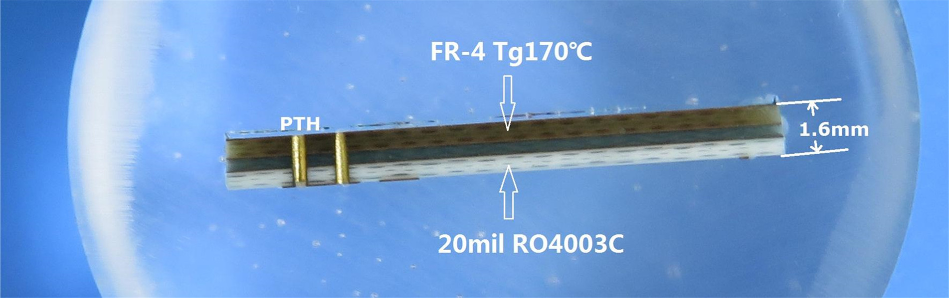
A hybrid stack looks elegant on a cross-section drawing. It promises the low-loss, tightly controlled RF behavior of a ceramic-loaded hydrocarbon laminate on the outer layers, and the cost and processing familiarity of an FR-4-type low-loss material in the middle. On paper, that is exactly what an 8-Layer RO4350B MT40 Hybrid PCB delivers: two 0.168 mm (6.6 mil) Rogers RO4350B cores at the outer sub-stacks, two 0.381 mm Isola I-Tera MT40 cores and three 0.12 mm MT40 prepreg bonds in the center, pressed to 1.636 mm with L1–L2 and L7–L8 blind vias.
What the drawing does not show is the press. Three different dielectric constructions are being laminated together, and almost every field failure of a board like this—delamination, bow and twist, inner-layer shift, or a 50Ωline that drifts out of tolerance—is decided during lamination, not routing. The three issues below are the ones a process engineer actually has to solve, together with the controls that make the build repeatable.
1. Two different CTE curves share one panel
The two materials are not dimensionally identical. RO4350B lists a coefficient of thermal expansion of 10, 12 and 32 ppm/°C in the X, Y and Z axes over−55 to 288°C, while I-Tera MT40 lists about 12 ppm/°C in-plane, 55 ppm/°C through the thickness below its glass transition, and 290 ppm/°C above it. The in-plane figures are close, which helps, but the z-axis values differ and the two resins soften at different temperatures—RO4350B's Tg is above 280°C by TMA, while MT40's is about 215°C by DSC. During a fast press, the MT40 relaxes through its resin-flow window while the RO4350B behaves differently; cool too quickly and the mismatch is locked in as residual stress that appears as warpage or delamination.
The improvement is a segmented, gradient profile rather than a single fast ramp. The MT40 processing window calls for a controlled 3.0–5.0°C/min heat ramp, a vacuum dwell with product temperature held below 100°C, a defined flow window at 100–140°C, and a cure near 200°C (not exceeding 210°C) for roughly 60 minutes. Equally important is the cooling side: cool at about 2.8°C/min down to 135–140°C under residual pressure before releasing the load. The symmetric build—an MT40 core and prepreg mirrored about the center and identical RO4350B cores on both faces—is the structural condition that lets the staged ramp and slow cool cancel shrinkage rather than accumulate it.
Inner layers receive a reduced-oxide or oxide-alternative treatment with uniform coverage, and drilled holes are desmeared using parameters suited to a 170 Tg FR-4 system—two passes for high-reliability boards over 2.5 mm—so plated copper anchors into a clean surface. MT40's total z-axis expansion is held to 2.8% from 50 to 260°C, and a T260 time-to-delamination greater than 60 minutes gives a measurable margin before the interface is at risk.
2. A thick 1.636 mm panel amplifies registration error
A 1.636 mm eight-layer board is a thick, four-core package, and it is laminated more than once because the L1–L2 and L7–L8 blind vias require sequential lamination. Each lamination cycle is an opportunity for resin flow and pressure to move an inner layer, and the error is cumulative: small slippage in the subassembly is carried into the final press. Non-uniform pressure makes this worse, because thick and thin dielectrics do not compress at the same rate, and a poorly centered or cushioned panel sees more flow at one edge.
The practical fixes are mechanical and procedural. Tooling holes are supplemented with registration targets on the inner layers and panel border, so blind-to-inner-land alignment is measured as a first-article dimension rather than found at final test. Lamination uses flat, parallel plates with calibrated cushion pads to even pressure, applied in stages after the vacuum dwell rather than as one full-pressure slam, consistent with MT40's 325–375 PSI window. Because the material shrinks slightly after etch and lamination, artwork compensation factors are applied to the inner-layer images. Thick panels are drilled one high with conservative parameters, and registration is re-verified at every sequential lamination step rather than only at the end. Copper distribution is balanced on the two outer layers and around the border, because uneven copper pulls the panel asymmetrically while resin moves; the scrap rail carries comparable resin volume on both sides so flow is uniform before reaching the product. This keeps the cumulative shift from each cycle within the blind-via land tolerance rather than stacking unchecked.
3. A 6 mil 50Ωline is at the mercy of dielectric thickness
The top RF face uses a 6 mil single-ended microstrip controlled to 50Ωon a 0.168 mm RO4350B core. That geometry is defined as much by the dielectric height under the trace as by the trace width, and a stack that alternates thin 0.12 mm prepreg bonds with 0.381 mm cores is especially sensitive: a small absolute error on a thin bond is a large percentage of the gap, and the reference plane moves. Lot-to-lot Dk variation (RO4350B is 3.48±0.05; MT40 core and prepreg sit around 3.36 and 3.15) compounds it.
The control starts before the press. Incoming cores and prepreg are accepted against tighter thickness tolerances and held to defined glass styles and resin content, so bond thickness stays predictable; prepreg is stored at or below 23°C and under 50% RH so moisture cannot alter flow. Fabricators build with measured core thicknesses and keep to specified glass styles rather than substituting equivalents. Impedance is then confirmed rather than assumed: dedicated coupons on each production panel are measured by time-domain reflectometry, and the layup or line width is adjusted against coupon data before volume release, which keeps the 50Ωresult repeatable across lots instead of only on the first article. Foil choice matters at the same order as thickness: HVLP or reverse-treated foil lowers the surface-roughness contribution that otherwise adds loss on an exposed RF line. Where the line is covered by solder mask, the mask's added dielectric is compensated in the model rather than ignored. Field-solver work uses the design Dk rather than the process value, which removes a common source of first-article error.
The result is a process-controlled product
An 8-Layer RO4350B MT40 Hybrid PCB is not difficult because the materials are exotic. It is difficult because one press must reconcile three dielectric constructions, two CTE curves, a thick 1.636 mm package and a tightly controlled 50Ωline. The solutions are not exotic either: a segmented ramp with slow cooling, registration targets and pressure uniformity for the sequential build, and tight incoming-thickness control backed by TDR coupons. Executed within those windows, it becomes a repeatable hybrid rather than a lucky one—the difference between a board that passes over production and one that only looks correct on the drawing.
Categories
New Blog
Tags
 6-11C Shidai Jingyuan, Fuyong, Baoan, Shenzhen, Guangdong, China 518103


For inquiries about our products or pricelist, please leave to us and we will be in touch within 24 hours.
© Copyright: 2026 Shenzhen Bicheng Electronics Technology Co., Ltd.. All Rights Reserved.

IPv6 network supported


