Why People frequently want to know about the hybrid circuit? This is due to the development of technology. When making electronic products, the hybrid circuit is useful. Understanding how this component functions in technical gadgets and electronic equipment is absolutely essential. The significance of the hybrid circuit is the main topic of discussion. What are the advantages of hybrid circuit components?
The goal of this page is to address all queries regarding the hybrid circuit. The advantages of hybrid PCB would be emphasized more. You will also discover the benefits of its parts and how to use the hybrid circuit. Soldering enables these tiny components, which are made possible in technical instruments.
Hybrid technology appears to be being used more frequently in our electronic devices as technology advances. Prepare to learn fresh and fascinating things about the hybrid circuit as you read this article. You hold the appropriate part in your hands.
What Is a Hybrid Circuit?
It is imperative to emphasize more what a hybrid circuit is. This section of the essay concentrates on the essential information about hybrid circuits.
The components of modern electronic equipment make it simpler to install this circuit. The technological components had a variety of installation procedures when electronic technology was still in its infancy. These parts were essentially anchored to or attached to metal enclosures. These metal boxes were fastened together with cables and secured with screws.
These technological components are heavy and bulky in today's world. They primarily discharge large amounts of power in thermoelectric device mode. Better technologies had to be necessary because of this. Transistors and other microscopic electronic components were created as a result of this. These are now known as printed circuits.
A type of printed circuit is the hybrid circuit. This consists of electronic devices with tiny element sizes. Soldering is used to join this component to the cushioning board. A hybrid polygonal printed circuit board (PCB) is one that makes use of various kits. The purpose of this is to increase electrical discharge.
Additionally, it aims to improve system accuracy for extremely high periodicity RF applications. Controlling the various quantity of caloric enlargement (CTE) tract of the diverging orbit materials is the major conflict experienced when constructing this type of PCB. Not only through PCB fabrication, but also through component abundance.
When creating a PCB with different equipment, there is something very crucial to keep in mind. You must have adequate training in both the foil's remarkable components and your apparatus's capability. Something occurs as a result of the CTE value of these chemicals' loop. During aerial heated uncovering or lamination, each substance grows to a different extent. This can be the reason for weighty registration challenges as a material diminishes while another substance amplifies.
Additionally, this can cause the copper covering on the connecting to peel off. But not all materials can be used in hybrid applications. This is thus despite the preferred or desired implementation, not all can be manufactured. Using one's PCB fibber quickly during design process can lead to reaching unheard-of results because one is aware of the types of materials that can be combined most effectively.
The growth of Very Large Scale Integration circuits and the steady decline in the size of inert components like capacitors over the past few years have ushered in new automation and breakthroughs like the SMD. Modern modern hardware's reduced bulk is made feasible via SMD. Thus, it helps with an increase in operations as well as power utilization.
It is better to refer to the hybrid circuit as cushioning equipment in order to continue the discussion. Through the use of some photolithography processes, the ceramic panel that serves as this insulating component enables the integration of passive devices. Above all, it uses particular inks. It is quite tiny as a result.
An integrated circuit and certain printed circuits together make up a hybrid circuit, a type of automation. Surface mount devices, also known as SMDs, and every other kind of technology are sucked up by this technology. Additionally, it fixes bugs and saves its extra advantages.
The pricing of hybrid circuits were once prohibitive when they were first released. Only large organizations, like aerospace, were able to access it as a result. The cost can also be covered by the military. Even though hybrid circuits are pricey nowadays, people from all different backgrounds can purchase them. Competitive pricing is used.
How Is The Hybrid Circuit Formed?
We mentioned before that the hybrid circuit is covered in this article. Understanding how the components are made is crucial. The ceramic composition of the hybrid circuit is good. It is able to absorb the proper component of power thanks to the assistance it receives from this ceramic plate. The hybrid circuit's superficial backing is provided by the ceramic plate. This component has exceptional thermal pressure or strength and strong mechanical insulation properties. It is therefore suitable for these types of operations.
The resistor is integrated into the outside, and a particular resistive patch is applied on it using a photolithography technique. The molecules that make up the resistive patch are highly elegant conductive alloy molecules. These molecules might be silver or gold. Therefore, some gum is used to cement it together. This depends on the molecules that make up those units as well as the density and expansion of the hoof prints. Without necessarily adhering to popular values, one can obtain a sizeable amount of inherent resistance value. One can utilize a bar to create a lovely split on it in order to change the resistivity value. The termination alloy wire will aid to vaporize as a result.
The resistance's intrinsic value can increase thanks to these adjustments. It is not required to reduce any resistance value. The resistor typically has some secondary resistance value when you are designing it. It has to do with changing the resistance value as the design develops.
The condensing shoal is where the electrical condensers are joined. They can be identified from one another by the silicon dioxide-based cushioning adhesive. This strategy might not always be successful in mass production. This is the main justification for the widespread adoption of various elements or SMD external stake.
The technological fragments are made of gold and platinum-based conductive ink. Given that it is highly challenging to make hybrid circuits function with exceptionally elegant ceramics, they could be referred to as unilateral circuits. However, in the main design and production, it is simple to build some "bridges" alongside numerous layers.
The availability of high-quality circuits is no longer disputed in the present. Because of this, straightforward hybrid circuits are common. These straightforward hybrid circuits are offered by many electronic departments. They combine different standard applications that are frequently used by the general public. The typical audio transmitters, receivers, and data are not far from these applications.
It is interesting that some electronic gadgets can be plotted and gathered thanks to receiver and transmitter components. To function properly, these components do, however, essentially require some generated power.
When they are in an orbit between 12 and 18 volts, the battery will occasionally electrify them. With some TTL reasoning rankings or placements, the data conductor components are compatible. To convert some microphone waves, the audio conductor can connect to an LF converter. These circuits enable numerous firms to utilize technology more efficiently today, saving PCB space.
What Are The Advantages Of Hybrid Circuits?

The advantages of hybrid circuits are numerous. The following are these merits:
Through design, the ultimate conduit value is determined. It's interesting that laser neatening can control or modify it.
A number of recent advancements in composite circuitry, such the LTCC-substrate composite, allow for the implantation of elements into the surfaces of a multidimensional coating in relation to elements that are positioned on the coating's layer.
In an unsolvable IC, elements that seem impossible to add can be used. These include inductors, diamonds, winding elements, and extremely valuable capacitors.
Regarding the choice of rheostat value in compact film technology, the orbit developer has complete autonomy.
To produce the desired values, the creation and proportion of the rheostat can be chosen.
Regulating before the ultimate test probably can be affected by diligent laser embellishments.
The constant use of the compact film aids the merit of its ingenuity.
What Is a Hybrid Integrated Circuit?
There is no denying that the hybrid integrated circuit is a topic of interest. To put it another way, the majority of people believe that a hybrid integrated circuit and a hybrid circuit have different properties. Let's give a brief explanation of this.
So, when we talk about a hybrid circuit, we're talking about one of the components on a printed circuit board. Similar to any monolithic integrated circuit, this is how it works. All hybrid circuits and hybrid integrated circuits, however, have significant and noticeable differences.
The obvious differences between the devices may be found in their design and construction. The installations and constructions of the two devices differ. However, both are really small. Specific components, including passive devices and some semiconductor components, make up the HIC. Transistors and monolithic ICS are semiconductors, while capacitors, inductors, and transformers are passive devices.
As a result, it is believed that no printed circuit board that contains components from another PWB can be considered to be a natural hybrid circuit. This is compatible with the MIL-PRF-38534 principle. The monolithic IC is in related to the integrated circuit.
The hybrid integrated circuit, which uses a variety of applied technologies, is a complete electronic perimeter built around a padded knockoff. The coating acts as a conduit for the boundary. As a result, it has the corresponding hoofprints of the device carved using polygonal techniques on it.
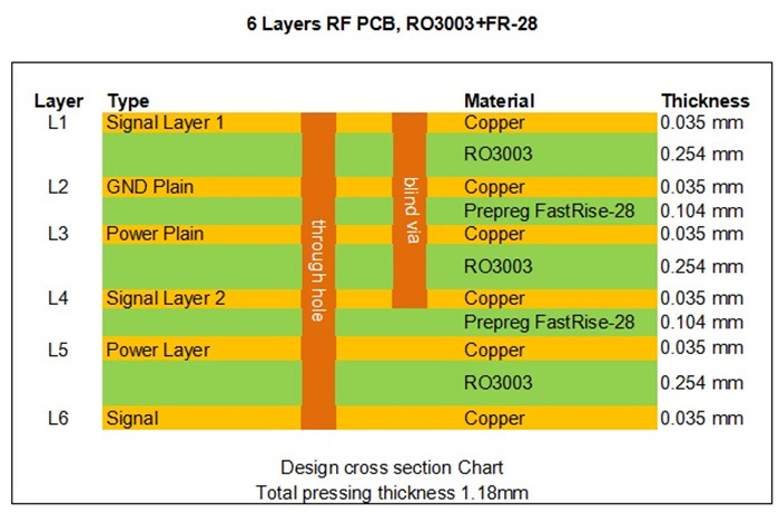
Different materials are used to construct the substrate core layers and the dielectric layers of a
hybrid printed circuit board. The construction of a hybrid PCB uses a variety of materials as opposed to just one. Different materials are employed to minimize any potential drawbacks of a certain material and incorporate all positive aspects into the PCB manufacturing process.
Outstanding strength, improved signal performance, and a more steady dielectric constant are possible benefits. Poor heat transfer, a low coefficient of thermal expansion, and other drawbacks of these materials may exist. In order to strengthen system dependability and enhance electrical performance, hybrid PCB materials that are different from one another.
Due to this manufacturing process, this type of PCB is used in high-frequency Radio frequency applications. One of the greatest challenges that come with producing this type of board is handling the various CTE properties of the different circuit materials during the component assembly and PCB production. `
The fabrication of Hybrid PCB involves the use of PTFE laminates and FR-4 material. When designing a hybrid PCB, it is very important to know the appropriate materials used for it. The Polytetrafluoroetyhlene laminates and FR-4 material help to condense RF functionality on the PCB and as such, reducing the costs of the device.

Materials Utilized in the Fabrication of Hybrid PCBs
PTFE and FR-4 are the two main materials used in the construction of hybrid PCBs. Multiple laminates made of the same material, such as PTFE lamination filled with ceramic, may be present in the layers of these PCBs. To make the materials functional for specific purposes, the designer will need to modify some of the material's formula in order to create various dissipation factors and dielectric constant rates.
PTFE
A plastic with ceramic filler used to create high-frequency PCBs is called PTFE material. This material's high dielectric constant makes it suited for uses that call for less signal loss and better impedance control. Due to its excellent mechanical stability, polytetrafluoroetyhlene is a type of material that is also used for applications that will be exposed to higher temperatures.
However, because it is a more expensive choice, PTFE has its own drawbacks. Being a softer material, it will also go through dimensional changes.
FR-4
A printed circuit board is frequently made out of a material called FR-4. The PCB industry holds this substance, sometimes referred to as Flame Retardant 4, to a high level. Its inexpensive expenses are mostly responsible for its popularity. This substance has excellent dielectric strength and electrical insulation. The material FR-4 is resistant to moisture and changes in temperature.
This material is beneficial in a range of applications because of its properties. Although this material has some drawbacks, it is still a good choice. The characteristics of this material preclude their suitability for recently produced higher frequencies.
Polyimide
Another sort of material that can be utilized to create a hybrid circuit is polyimide. Because of their strong chemical resistance, these materials can withstand some chemicals. Aside from this characteristic, polyimide has excellent electrical characteristics and can be applied in a variety of ways.
For portable applications, polyimide is a lightweight, flexible material. However, due to its higher price compared to PTFE and FR-4, polyimide is a less popular alternative.
Why are Different Materials Used for Designing Hybrid PCB?
The different materials utilized in the production of hybrid printed circuit boards is one of their distinctive characteristics. For various purposes, materials that are dissimilar are used. The main goal of using various materials to create multilayer boards is to lessen some of the laminates' poor structural and mechanical properties.
When these laminates are put together, they balance one another out by minimizing certain materials' drawbacks and enhancing others' strengths. For instance, PTFE has excellent electrical qualities but when exposed to certain temperatures, it may suffer from structural difficulties.
Combining several materials also aids in lowering fabrication costs, making it a cost-effective choice. Hybrid PCBs are typically designed using PTFE and FR-4. For high-speed applications, PTFE laminates are used, although FR-4 has sufficient advantages for low-speed ones. Furthermore, the thickness problems for the layers of these laminates can be balanced using FR-4 materials.
Issues to Consider when Designing Hybrid PCBs
When creating a circuit board that uses various materials, there are a few aspects that need to be taken into account. It's critical to realize that the CTE values of various materials vary. The numbers show how much each material's dimensions will change when subjected to various temperatures.
As a result of one laminate expanding while another shrinks, registration problems may arise. It is crucial to remember that some materials are inappropriate for use in hybrid applications. When creating multilayered hybrid PCBs, layer separation is a significant issue that needs to be resolved. Another potential problem is delamination. In this situation, the laminate layers start to separate.
Understanding the time a material will delaminate is crucial for combating the problem. Another significant problem encountered when building hybrid PCBs is the stack-up procedure. In order to fulfill the requisite thickness without impacting the acceptable frequencies, fabricators must have the correct thickness for the circuit board for every piece and panel. The adhesive technology used for hybrid circuit boards differs based on the materials used. The right quantity of insulation will ensure that the printed circuit board is the proper thickness.
Not all businesses have the knowledge or expertise needed to design hybrid PCBs. Some materials may be used by PCB fabricators. The fabricator must also be aware of a few problems that can arise when etching multilayer boards.
When Should Hybrid PCB Stackup be used?
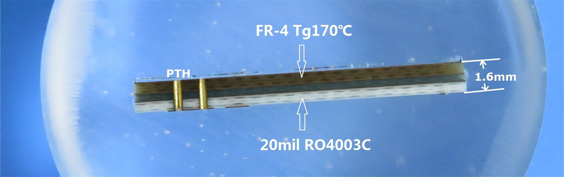
hybride Rogers + FR4 material
When to employ hybrid PCBs depends on a number of variables. Some of these variables include prices, temperatures, application functions, and frequency. One advantage of hybrid PCB stackups is that they give you more creative freedom when creating a circuit board with the necessary mechanical and electrical properties.
When it comes to hybrid designs, cost considerations are also crucial. You can profit from utilizing a less expensive material in areas where higher frequencies aren't needed since hybrid PCBs use different types of materials. For the parts of the PCB that require greater electrical, thermal, and mechanical qualities, you can then utilize a lower amount of the costly materials.
Mechanical Features of a Hybrid PCB
During the fabrication of Hybrid PCB, some PCB designers desire some unique mechanical features that may be complex to include. Some of the features are
Odd shape board outlines
The printed circuit board occasionally has distinct bends and twists, and the laminates typically have to fit into other spaces. The PCB's outline routing for a hybrid design is a delicate process. To keep the edges sharp, the speeds and feeds must be lowered.
Since the material is more complicated on drill bits, it is also crucial to keep an eye on your drill bits. Additionally, you should be aware that if they are not cut properly, the majority of RF fabrics can fray easily.
Plated through hole consistency
A fabricator must understand that hole preparation before plating for FR4 is different. The way these processes affect the quality of the hole wall must be understood. For PTFE, you must use plasma etch process to desmear the holes. This is not the ideal method for FR4 as it can result in an uneven surface which will then lead to uneven copper in the holes.
Controlled depth rout process
A regulated depth routing pattern results in some mechanical characteristics of hybrid PCBs, while many lamination cycles produce others. However, these procedures have their own issues that might make the PCB design more complicated and expensive.
When using multiple lamination cycles to construct these cavities, a manufacturer must route out the production pattern as well as the design in the prepreg.
What Are The Features Of Hybrid PCB?
This is one of the inquiries about the hybrid circuit that is asked the most frequently. It is crucial to take note of a circuit's characteristics. You fully comprehend how it is built if you are aware of all of its parts. You not just comprehend its composition but also comprehend how it functions most effectively. Hybrid circuits have been the subject of several discussions.
Simply said, the hybrid PCB is a versatile component. The only goal of this PCB's utilization of several dissimilar components is to improve electrical performance. The hybrid circuit's PCB is a compact board. It is an electronic circuit with elements of more than one kind or category.
Where Are Hybrid Circuits Used?
People would constantly be interested in learning more about the hybrid circuit. Understanding hybrid circuits' uses is essential. The parts of this circuit have already been covered in great detail. Now let's think about the applications for hybrid circuits.
The majority of circuits in use today across all industries are hybrid ones. They are mostly used when mechanical components must meet extremely high technical requirements.
Applications include everything from security and calming electronics to mechanisms and portable power fragments. One may clearly admit that only hybrids meet the high criteria when there is serious ecological chaos under the hood. The hybrid circuit's ability to integrate components that typically cannot be added to a standard monolithic IC is one advantage.
There are various gadgets that use the hybrid circuit. Diverse electrical equipment also contains various sorts of circuits. All of the electronic gadgets and equipment that we use on a daily basis contain components that revolve around these circuits.
These circuits are found in a variety of appliances, including laptops, phones, computers, refrigerators, and televisions. Without circuits, whether little or large in size, it is impossible to manufacture these electrical devices.
These devices' electrical circuits can be simple or complex when they're being made. These electrical circuits are created by connecting a number of electrical components together. This connection is made in addition to joining wires or conducting cables to allow mechanical current to be discharged through the various circuit components.
More Information on Hybrid PCB
When creating the hybrid printed circuit board, there may be various difficulties. It demands that one prepare for the performance. Conducting the diverging quantity of thermal extension (CTE) components of the various circuit parts during PCB construction as well as a component throng is one of the major issues manufacturers face.
It should be noted that these designs typically combine certain FR-4 components with PTFE laminates. This forces a fabricator to squeeze the pair of RF features onto an identical PCB, which can reduce the appliance's size and cost.
Engaging one’s PCB designer beforehand in the layout process will enable one to get the perfect after-effects. This is because the fabricators mostly have a vast knowledge of materials that can be blended. It is perceived that materials such as the Rogers 5880 are an extremely excellent RF property used in towering dependable applications.
The component's problem with getting smaller is the most difficult one. This is what remains after someone removes the copper. As a result, your designer needs to be more knowledgeable about the production's tasks. This will enable him or her to overcome the significant obstacle. Hybrid PCBs, hybrid microwave circuits, and hybrid microcircuits all provide production-related difficulties. This is not meant to diminish their efficiency in any way.
What Is The Innovative Idea Behind The Hybrid Circuit?
The hybrid circuit was developed primarily to advance our electronic technology. This is due to the circuit's small electronic size. Additionally, it employs a variety of elements. It is largely made up of passive materials and individual components. Hybrid circuits have advanced and become more inventive in recent years. Modern appliances and quantum computers both exhibit this. The hybrid circuit unquestionably has a big impact on the electronics sector.

 Call Us Now !
Tel : +86 755 27374946
Call Us Now !
Tel : +86 755 27374946
 Order Online Now !
Email : info@bichengpcb.com
Order Online Now !
Email : info@bichengpcb.com
 6-11C Shidai Jingyuan, Fuyong, Baoan, Shenzhen, Guangdong, China 518103


