
 Call Us Now !
Tel : +86 755 27374946
Call Us Now !
Tel : +86 755 27374946
 Order Online Now !
Email : info@bichengpcb.com
Order Online Now !
Email : info@bichengpcb.com
RO4360G2 PCB: Features, Benefits, and Applications
Introducing the RO4360G2 PCB, a cutting-edge solution developed by Rogers Corporation. The 20mil RO4360G2 laminates are low loss, glass-reinforced, hydrocarbon ceramic-filled thermoset materials that strike the perfect balance between performance and processing capability. These innovative laminates are the first high dielectric constant (Dk) thermoset laminates that can be processed similarly to FR-4, offering enhanced rigidity and reduced material and fabrication costs. With lead-free process compatibility and superior performance, RO4360G2 laminates are the ideal choice for high-frequency applications demanding exceptional quality and reliability.
Features:
The RO4360G2 PCB boasts a range of remarkable features that contribute to its outstanding performance:
1.High Dielectric Constant (Dk): The PCB exhibits a dielectric constant of 6.15 +/- 0.15 at 10 GHz/23°C, ensuring precise signal integrity and reliable transmission.
2.Low Dissipation Factor: With a dissipation factor of 0.0038 at 10 GHz/23°C, the RO4360G2 PCB minimizes signal loss and provides exceptional high-frequency performance.
3.High Thermal Conductivity: The PCB possesses a high thermal conductivity of 0.75 W/mK, facilitating efficient heat dissipation and ensuring the reliability of temperature-sensitive components.
4.Excellent Thermal Stability: The RO4360G2 PCB features a high glass transition temperature (Tg) greater than 280 °C TMA, ensuring excellent thermal stability and compatibility with lead-free soldering processes. The Td value exceeds 407°C, further enhancing the PCB's resilience to high temperatures.
5.Low Coefficient of Thermal Expansion (CTE): The PCB offers a low Z-axis CTE of 28 ppm/°C, minimizing the risk of failures due to thermal stress and ensuring dimensional stability.
6.Copper-Matched CTE: The PCB exhibits copper-matched CTE values of 13 ppm/°C (X-axis) and 14 ppm/°C (Y-axis) in the temperature range of -55 to 288 °C, ensuring reliable interconnectivity and reducing the risk of delamination.
7.Lead-Free Process Compatible:The RO4360G2 PCB is compatible with lead-free processes, ensuring compliance with environmental regulations and providing an eco-friendly solution.
8.Flammability Rating: The PCB meets the 94V-0 flammability rating, offering enhanced safety and reliability.
Benefits:
Investing in the RO4360G2 PCB provides numerous benefits that make it an exceptional choice for a wide range of applications:
1.Design Flexibility:The RO4360G2 PCB offers design flexibility, allowing for complex circuit layouts and high-density interconnections.
2.Plated Through-Hole Reliability:The PCB ensures reliable plated through-hole connections, enhancing the overall robustness and longevity of the assembly.
3.Automated Assembly Compatible:The RO4360G2 PCB is compatible with automated assembly processes, facilitating efficient and cost-effective manufacturing.
4.Environmentally Friendly: With lead-free process compatibility, the RO4360G2 PCB contributes to environmentally friendly practices and compliance with regulations.
5.Efficient Supply Chain and Short Lead Times: The availability of the RO4360G2 PCB worldwide, combined with efficient supply chain management, ensures shorter lead times and cost-effective material options.

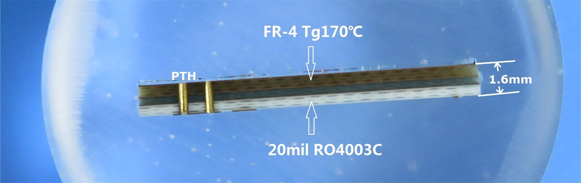
PCB Stackup and Construction Details:
The RO4360G2 PCB features a 2-layer rigid PCB with the following stackup:
Copper Layer 1: 35 μm
Rogers RO4360G2 Substrate: 20mil (0.508mm)
Copper Layer 2: 35 μm
The PCB construction details are as follows:
Board Dimensions: The PCB measures 68.35mm x 41.4mm, offering a compact and versatile solution for various applications.
Minimum Trace/Space: The PCB supports a minimum trace/space width of 4/6 mils, enabling intricate circuit designs and high-density interconnections.
Minimum Hole Size: The PCB accommodates a minimum hole size of 0.35mm, allowing for the integration of various components and efficient assembly processes.
No Blind Vias: The absence of blind vias simplifies the manufacturing process and reduces production time and costs.
Finished Board Thickness: The finished board thickness is 0.6mm, striking a balance between durability and flexibility for diverse applications.
Finished Copper Weight: The outer layers of the PCB have a finished copper weight of 1 oz (1.4 mils), ensuring excellent conductivity and signal integrity.
Via Plating Thickness: The via plating thickness is 20 μm, providing reliable interconnectivity and ensuring robust performance.
Surface Finish: The PCB is coated with immersion gold, which offers excellent solderability, superior flatness, and corrosion resistance.
Top Silkscreen:The RO4360G2 PCB does not have a top silkscreen layer.
Bottom Silkscreen: The RO4360G2 PCB does not have a bottom silkscreen layer.
Top Solder Mask: The top solder mask is blue, providing protection and insulation for the PCB traces.
Bottom Solder Mask: There is no solder mask on bottom layer.
100% Electrical Test: Each RO4360G2 PCB undergoes a rigorous 100% electrical test before shipment, guaranteeing optimal performance and reliability.
Filled Vias: The PCB features 0.5mm filled vias, which are filled with resin and capped, enhancing their structural integrity and ensuring consistent electrical connectivity.
PCB Statistics:
The RO4360G2 PCB specifications include the following statistical data:
Components: The PCB supports up to 11 components, allowing for diverse circuit configurations and functionalities.
Total Pads: The total number of pads on the PCB is 70, ensuring sufficient connectivity options for component integration.
Thru-Hole Pads: The PCB features 46 thru-hole pads, enabling reliable connections and secure component mounting.
Top SMT Pads: The PCB offers 24 top surface-mount technology (SMT) pads, allowing for efficient placement of SMT components.
Bottom SMT Pads: The RO4360G2 PCB does not have bottom SMT pads.
Vias: The PCB includes 35 vias, providing ample options for interconnectivity and signal routing.
Nets: The PCB supports 3 nets, ensuring efficient and organized signal distribution.
Type of Artwork Supplied:
The RO4360G2 PCB accepts Gerber RS-274-X artwork, enabling seamless integration into existing design and manufacturing processes.
Accepted Standard:
The Rogers 4360G2 PCB adheres to the IPC-Class-2 standard, ensuring high-quality manufacturing processes and reliable performance.
Availability:
The RO4360G2 PCB is available worldwide, allowing customers from various regions to benefit from its exceptional features and performance.
Some Typical Applications
The versatility and high-performance characteristics of the RO4360G2 PCB make it suitable for a range of applications, including:
1.Base Station Power Amplifiers: The RO4360G2 PCB provides excellent signal integrity and thermal management, making it an ideal choice for base station power amplifiers in wireless communication systems.
2.Small Cell Transceivers: With its low loss and high thermal conductivity, the RO4360G2 PCB is well-suited for small cell transceivers, ensuring reliable and efficient data transmission in compact wireless communication devices.
In conclusion, the Rogers RO4360G2 PCB offers an exceptional combination of performance, processing capability, and design flexibility. With its high dielectric constant, low dissipation factor, excellent thermal stability, and lead-free process compatibility, it meets the demands of high-frequency applications while providing environmentally friendly features. The RO4360G2 PCB's availability worldwide, efficient supply chain, and short lead times further enhance its appeal. Whether used in base station power amplifiers or small cell transceivers, the RO4360G2 high frequency PCB ensures optimal performance, reliability, and cost-effectiveness, making it the ideal choice for advanced electronic designs.
Categories
New Blog
Tags
 6-11C Shidai Jingyuan, Fuyong, Baoan, Shenzhen, Guangdong, China 518103


For inquiries about our products or pricelist, please leave to us and we will be in touch within 24 hours.
© Copyright: 2026 Shenzhen Bicheng Electronics Technology Co., Ltd.. All Rights Reserved.

IPv6 network supported


