
 Call Us Now !
Tel : +86 755 27374946
Call Us Now !
Tel : +86 755 27374946
 Order Online Now !
Email : info@bichengpcb.com
Order Online Now !
Email : info@bichengpcb.com
What makes TP2000 PCB outperform FR‑4 at 5GHz and radar applications?
What makes TP2000 PCB outperform FR‑4 at 5GHz and radar applications?
Meta Description:
TP2000 PCB offers a uniqueultra-high dielectric constant (Dk=20) and ultra-low dissipation factor (Df=0.002) for compact RF and microwave designs. Learn why this thermoplastic material outperforms conventional laminates in antenna, radar, and satellite systems.
When you first look at a TP2000 high frequency PCB specification sheet, two numbers usually jump out: dielectric constant (Dk) of 20 and a board thickness of 6.1mm. In an industry dominated by FR-4 (Dk~4.5) and standard high-frequency materials like Rogers (Dk~3.5–10), a Dk of 20 sounds almost extreme.
But extreme performance is exactly what many RF engineers need today. The challenge? Most PCB suppliers either don’t understand how to fabricate such materials, or they present the specs in a dry, intimidating table that scares away potential buyers.
This blog is not another datasheet. Instead, let’s walk through the real engineering problems that TP2000 PCB solves, why its unusual construction makes sense for miniaturized high-frequency circuits, and how you can confidently specify it for your next antenna or radar project.
The Hidden Cost of Miniaturization
Every RF designer faces the same physical constraint: wavelength shrinks as frequency increases, but component sizes and tolerances do not. At 5 GHz, the free-space wavelength is about 60 mm. On a standard FR-4 board, the guided wavelength becomes roughly 28 mm. To build a functional patch antenna, phase shifter, or filter, you still need a certain electrical length—oftenλ/4 orλ/2.
With a conventional Dk of 3 to 10, your traces and resonators take up significant board real estate. In phased array antennas with 64 or 128 elements, that real estate becomes a cost and weight nightmare. The instinct is to increase Dk to shrink the design. But most high-Dk PCB materials come with a painful trade-off: high dissipation factor (Df), poor thermal stability, or terrible machinability.
This is where TP2000 enters the stage—not as a“me too”material, but as a genuinely different solution.
What Makes TP2000 Different ?(Without the Marketing Hype)
Let’s start with the core facts from the actual product construction you received:
Material system: Ceramic-filled polyphenylene oxide (PPO) thermoplastic, no glass fiber reinforcement.
Compared to ceramic-filled PTFE laminates (common at high Dk), the PPO-based TP2000 offers two practical advantages: better dimensional stability during temperature cycling and much easier machining. No glass fiber means no frayed edges, less drill wear, and no special plasma treatment for via walls.
Compared to standard FR-4? The Df of FR-4 at 5 GHz is typically 0.015–0.025—an order of magnitude higher. That difference translates directly into insertion loss. In a 4-stage filter or a long feed network, switching from FR-4 to TP2000 can cut dielectric loss by 85–90%.
The“6mm Thick, No Solder Mask”Design–Why It Works
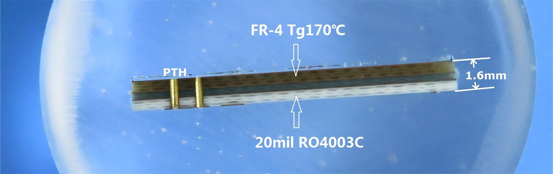
One of the most surprising details in the TP2000 PCB specification is the finished board thickness: 6.1 mm for a 2-layer rigid board. Most RF PCBs are 0.8 mm to 1.6 mm thick. Six millimeters sounds like a mechanical support layer, not an RF substrate.
But here’s the engineering logic:
With a Dk of 20, the electrical thickness of a 6 mm board is equivalent to an FR-4 board of about 1.35 mm in terms of electrical phase length. However, the mechanical rigidity is much higher. This is intentional for applications like:
Heavy copper antenna elements (1 oz / 35 µm is standard, but the board can handle higher current without flexing).
Direct mounting of RF connectors and power amplifiers without additional stiffeners.
Vibration-resistant designs in aerospace and defense systems.
Also note: No top or bottom solder mask, no silkscreen. That’s unusual for a standard PCB, but perfectly logical for high-frequency work. Solder mask has its own Dk and Df (usually poor, around 0.01–0.02 Df). At 5 GHz and above, even a thin mask layer disturbs impedance and adds loss. Bare copper finish means you get predictable, low-loss transmission lines.
The via plating thickness is specified as 20μm–standard IPC Class 2. With 12 vias and only 2 nets, this is an extremely simple electrical network. That tells us the board is likely a passive RF component: a power divider, a delay line, or a custom antenna array. The simplicity of the netlist (just two nets) contrasts with the complexity of the material–a classic sign of a high-performance RF part where layout is everything.

From Spec Sheet to Real-World Application
Let’s be honest: a PCB with 24 components, 37 pads, and only 2 nets does not look impressive in a bill of materials. But that’s exactly the point. In RF engineering, performance is not measured by component count. A single resonant structure made from TP2000 can replace a multi-layer ceramic filter or a bulky cavity.
Consider these typical applications from the datasheet, but reinterpreted with practical benefits:
1. Phased Array Antenna Elements
A Dk of 20 allows you to reduce the patch size by a factor of about√(20/4.5)≈2.1 compared to FR-4. For a 5 GHz array, a single patch goes from ~14 mm to ~6.7 mm. That means you can double the element density or shrink the entire aperture by half. No other standard material gives you that size reduction without using expensive ceramic blocks.
2. Radar Systems (Automotive 77 GHz or Defense X-Band)
Dissipation factor of 0.002 at 5GHz scales well to mmWave (typical increase is only 0.0005–0.001 per decade). Low Df plus no glass fiber weave means low phase noise and stable group delay. For FMCW radar, that translates to fewer false targets.
3. High-Power RF Amplifiers
The operating temperature range of–100°C to +150°C and a Z-axis CTE of only 40 ppm/°C means excellent reliability under thermal cycling. The 6 mm thickness also acts as a heat spreader, though careful via design is needed to conduct heat to the bottom copper layer.
4. Satellite Communication Equipment
Radiation resistance is directly mentioned, and the thermoplastic PPO system holds up better than many thermosets under gamma and electron exposure. For LEO satellite transceivers where weight and stability matter, the 6.1 mm board can serve as both substrate and chassis.
Fabrication Realities–What Your CM Needs to Know
As a PCB supplier, you must address fabrication challenges head-on. TP2000 is NOT an ordinary material, but it is machine-friendly compared to PTFE ceramics. Here’s what we’ve validated based on the construction details provided:
Drilling: Standard carbide drills work fine. No glass fibers means minimal burring. Recommended speed slightly lower than FR-4 to avoid overheating the thermoplastic.
Via plating: The 20μm copper plating is achievable with standard electroless copper + electroplating. No sodium naphthalate etching or plasma treatment needed–a major advantage over PTFE.
Surface finish: Bare copper requires anti-tarnish protection before assembly. Recommend IPC-1601 handling or a temporary organic solderability preservative (OSP)–but that would add a thin dielectric layer. For RF purity, many customers prefer flash immersion silver or gold. However the spec says Bare Copper, so ship with a nitrogen-purged bag and desiccant.
Lamination: 2-layer, 6 mm total thickness implies a single thick TP2000 core, not multiple prepreg layers. That’s good for consistency. The outer copper is 35μm standard foil, not reverse-treated. This is fine for most microstrip designs up to 10 GHz.
No solder mask, no silkscreen: This simplifies fabrication and removes all lossy dielectrics from the signal path. It also means the board looks“raw” –educate your customers that this is by design, not a defect.
Electrical test: 100% tested before shipment. With only 2 nets, this is fast and effective.
When Should You NOT Use TP2000?
TP2000 is not a universal replacement:
Multilayer boards –The spec says no blind vias and only 2 layers. Complex 8+ layer designs would be difficult with thermoplastic PPO because of bonding and temperature sensitivity during multiple lamination cycles.
High-speed digital (e.g., PCIe, DDR)–Dk=20 is far too high for impedance-controlled digital lines. You’d need absurdly narrow traces (under 0.1 mm) to get 50 ohms, and propagation delay would be huge.
Cost-sensitive consumer products–TP2000 is specialty material. Expect pricing similar to high-end Rogers or Taconic, not FR-4.
Assembly with lead-free reflow–Peak temperatures of 260°C are acceptable (PPO melts >280°C), but multiple reflows may degrade the resin. Hand-soldering with a temperature-controlled iron is safer.
If you are designing a compact, high-performance RF or microwave circuit that operates up to 10–15 GHz, and you need to drastically shrink size without sacrificing loss, TP2000 DK20 high DK PCB is a serious candidate. The combination of Dk=20, Df=0.002, 6 mm rigid construction, and glass-free machinability is rare.
Don’t let the unusual specification (no mask, no silk, thick core) scare you. That’s not a compromise–it’s a deliberate optimization for RF performance. And as a supplier, we are ready to deliver these boards with 100% electrical testing, worldwide, meeting IPC Class 2.
So next time you struggle to fit an antenna array into a tight enclosure or fight excessive loss in a long feed line, remember: Sometimes the best solution looks nothing like a typical PCB. And that’s exactly what TP2000 is built for.
Need a quote or design review for your TP2000 PCB project?
Contact our team with your Gerber files (RS-274-X) and your stackup requirements. We support quick-turn fabrication of high-Dk, high-thickness boards for defense, aerospace, and telecom applications.
Categories
New Blog
Tags
 6-11C Shidai Jingyuan, Fuyong, Baoan, Shenzhen, Guangdong, China 518103


For inquiries about our products or pricelist, please leave to us and we will be in touch within 24 hours.
© Copyright: 2026 Shenzhen Bicheng Electronics Technology Co., Ltd.. All Rights Reserved.

IPv6 network supported


