
 Call Us Now !
Tel : +86 755 27374946
Call Us Now !
Tel : +86 755 27374946
 Order Online Now !
Email : info@bichengpcb.com
Order Online Now !
Email : info@bichengpcb.com
What the Datasheet Doesn’t Tell You About the 4-Layer WL-CT330 PCB?
What the Datasheet Doesn’t Tell You About the 4-Layer WL-CT330 PCB?
Meta Description:
Discover why the 4-layer WL-CT330 PCB is a practical choice for RF and high-speed designs. We go beyond typical specs to explore hybrid stackup decisions, thermal reality, and cost-conscious DFM.
When an RF engineer first looks at the datasheet for a 4-layer WL-CT330 PCB, the numbers jump out immediately: Dk of 3.30 at 10 GHz, dissipation factor of 0.0026, and a glass transition temperature above 280°C. Impressive, yes. But seasoned designers know that a laminate datasheet is only the starting point. What matters is how the material behaves inside a real multilayer stackup, how it survives assembly, and how consistently it delivers in the field when nobody is looking at a network analyzer in a lab.
This article steps away from the typical specification table. Instead, we examine what fabricators and design teams actually encounter when committing to a 4-layer WL-CT330 PCB—the trade-offs, the hidden strengths, and the questions worth asking before you finalize your Gerber files.
Why a 4-Layer Stackup with WL-CT330 and FR-4?
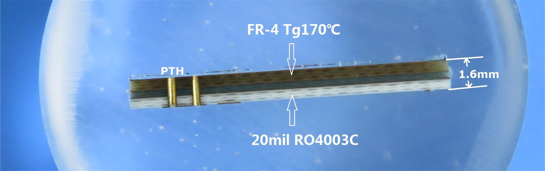
Hybrid constructions often make traditional RF designers nervous. Mixing a high-frequency hydrocarbon-ceramic laminate with a standardhigh-Tg FR-4 like S1000-2M sounds like a recipe for CTE mismatch or delamination. Yet the 4-layer WL-CT330 PCB covered here does exactly that: a 60 mil WL-CT330 core carries the critical RF traces on the outer layers, while a 31.5 mil S1000-2M core handles the inner ground and power planes, bonded by a 10 mil prepreg combination of 1080 and 7628 glass styles.
Why accept this mixed marriage? Cost and manufacturability. A pure WL-CT330 multilayer would push pricing beyond what many commercial 5G and automotive radar projects can tolerate. By placing the FR-4 core on inner layers—where dielectric loss matters far less—the stackup keeps high-frequency fields contained within thelow-loss WL-CT330 region. The result is a PCB that performs extremely close to a full RF laminate board but at a fraction of the cost. The S1000-2M core, with its own high Tg and reliable thermal performance, prevents the secondary material from becoming a reliability bottleneck.
One detail often overlooked: this particular 4-layer WL-CT330 PCB uses a prepreg combination of 1080 RC63% and 7628 (43%). That is not an arbitrary choice. The thin 1080 layer controls layer-to-layer registration and fills small topography, while 7628 provides mechanical stiffness. For minimum trace and space of 5/6 mil, the glass style matters—the last thing you want is resin-rich areas shifting your impedance on fine lines.

The Outer Copper Reality
The datasheet states finished copper weight: 1 oz on inner and outer layers. Fabricators achieve this by starting with 35μm copper foil and then plating an additional 20μm inside vias, which increases surface copper slightly beyond 1 oz after surface finish. That 20μm via plating thickness is robust enough for multiple reflow cycles and thermal shock, yet not so heavy that it wrecks fine-pitch geometries.
In a 4-layer WL-CT330 PCB carrying phased-array feed networks or high-speed differential pairs, copper thickness consistency is non-negotiable. Too much variation and your differential impedance walks away from 100Ω. The IPC Class 2 standard accepted here imposes a±20% tolerance on plated copper thickness. That is fine for digital and lower-frequency RF, but for millimetre-wave designs above 30 GHz, you would specify tighter control up front rather than assume the standard will be enough.
Thermal Stability That Goes Beyond Tg Numbers
Wangling WL-CT330 boasts a Tg above 280°C, T260 over 60 minutes, and T288 above 20 minutes. Those metrics look nearly indestructible compared to standard FR-4. However, the real question is how the complete 4-layer WL-CT330 PCB behaves under multiple lead-free assembly cycles at 260°C peak temperature.
The CTE values give a clue: X and Y CTE around 15 and 13 ppm/°C, Z-axis expansion at 39 ppm/°C. The S1000-2M material used for inner layers exhibits CTE values in a similar range, typically around 14-16 ppm/°C in X-Y and 45-55 ppm/°C in Z below Tg. This close match in X-Y CTE is what prevents the board from warping or developing barrel cracks in vias during reflow. Many designers only look at a laminate’s Tg and ignore CTE compatibility between different materials in the stackup. That oversight leads to field failures that never trace back to the datasheet’s headline number.
Another thermal detail: thermal conductivity of 0.59 W/m·K. Not a standout figure for heavy power applications, but entirely adequate for the typical RF power levels seen in automotive radar transceivers or small-cell base station amplifiers. If your design pushes continuous high power, you will want to complement the board with thermal vias and a metal-core or heatsink interface. The material itself will not be the limiting factor—the overall thermal design will.
Why Immersion Gold and Black Silkscreen?
The 4-layer WL-CT330 PCB described here uses immersion gold surface finish, green solder mask on both sides, and a top-side black silkscreen with no silkscreen on the bottom. That combination reveals a board intended for dense RF assemblies where soldermask-defined pads are the norm and where an aesthetic or contrast requirement exists—likely because the top side is visible or needs clear laser marking for traceability.
Immersion gold keeps the surface flat, critical for fine-pitch QFN or LGA packages and edge-mounted connectors. With a minimum hole size of 0.25 mm, the finish uniformity across small annular rings is important. ENIG also avoids the skin-effect losses that solder coating can introduce at higher frequencies. There is a minor insertion-loss penalty compared to bare copper or silver finishes, but for most designs operating below 30 GHz, the difference is negligible relative to the total loss budget.
The black top silkscreen on green solder mask is a functional choice: reference designator readability under varied lighting is actually better than white-on-green for some automated optical inspection systems. The absence of bottom silkscreen indicates the bottom layer likely carries a continuous ground plane with no components—the inner and bottom layers exist purely for power distribution and shielding.
Processing Simplicity: A Frequent but Critical Point
A significant reason designers migrate from PTFE-based materials to WL-CT330 is processability. The datasheet emphasizes that WL-CT330 processes like FR-4, not like PTFE. In a production context, that means no sodium etching, no specialized via preparation, and no risk of through-hole smear that requires plasma desmear cycles. The 4-layer WL-CT330 PCB can be manufactured on standard FR-4 lines, which both increases fabrication yield and shortens lead time.
The 100% electrical test before shipment, using flying probe or bed-of-nails methods, verifies net continuity and isolation. With minimum trace and space at 5/6 mil, the electrical test catches opens and shorts that visual inspection might miss at this density. For volume programs, the repeatability of this test is far more important than the initial coupon data.
Dk Stability When It Truly Counts
WL-CT330 Wangling PCB specifies dielectric constant at 10 GHz as 3.30±0.06, with a stable temperature coefficient of Dk (TcDk). Why does this matter? Consider a phased-array antenna operating outdoors where the board temperature can swing from -40°C to +85°C. A material with a large TcDk would shift the phase response of each antenna element with temperature, degrading beamforming accuracy. The stable TcDk of WL-CT330 allows calibration tables to remain simpler and beam patterns to hold across the temperature range without real-time compensation eating into processor overhead.
The dissipation factor of 0.0026 at 10 GHz places it in the same class as ceramic-filled hydrocarbon laminates that cost significantly more. Combined with the 1.524 mm core thickness, this Df yields insertion loss that is manageable for interconnects up to several inches at mmWave frequencies. When designers run link budgets for 28 GHz or 39 GHz small cells, they consistently find that the dielectric losses in a 4-layer WL-CT330 PCB leave enough margin for the active components and connectors—provided that trace launches and transitions are optimized.
What Application-Specific Details Matter?
The same 4-layer WL-CT330 PCB may end up in an automotive radar module, a 5G base station beamformer, or an aerospace telemetry transmitter. Yet the DFM priorities shift between these applications.
For automotive radar under-the-hood, moisture absorption of 0.05% maximum becomes a standout feature. In high-humidity environments, laminates that absorb moisture will see their Dk increase and Df climb, detuning the radar over its lifetime. WL-CT330’s near-zero moisture uptake means the radar stays aligned.
For satellite payloads, the combination of high volume resistivity (5×10⁹Mohm·cm) and UL 94-V0 flammability rating addresses outgassing and fire safety concerns that go beyond basic PCB performance.
For networking and server backplanes operating at 112 Gbps PAM-4, the total thickness of 2.7 mm creates a stiff, mechanically stable platform with enough layers to route power and control while the high-speed lanes run on the top surface WL-CT330 layer. The absence of blind vias simplifies fabrication but limits routing density; teams that need higher density would step up to a 6-layer or greater design.
What to Ask Your Fabricator Before Ordering
Rather than blindly uploading Gerber RS-274-X files and expecting a perfect batch, experienced designers ask targeted questions:
Can you provide impedance test coupons built on the actual hybrid stackup, not just on a standard test vehicle?
What is the tolerance on the 1.524 mm WL-CT330 core thickness across a panel? (This directly affects 50Ωline width.)
Will the 1080/7628 prepreg combination cause any resin starvation on 1 oz inner copper planes?
Is the black silkscreen compatible with the immersion gold process without residue or bleed?
These questions are not the stuff of glossy brochures, but they separate reliable suppliers from the rest.
A Sensible Choice Hidden in Plain Sight
The 4-layer WL-CT330 hybrid PCB succeeds because it avoids extremes. It does not chase the absolute lowest Df in the industry, nor does it try to be the cheapest option available. Instead, it combines a genuinely low-loss RF dielectric with a conventional FR-4 processing workflow, a well-matched FR-4 core, and surface finishes that work across multiple market segments. That balance—rather than any single headline number—explains why designers return to it for 5G, automotive radar, satellite, and high-speed networking projects.
For engineers and procurement teams alike, the lesson is clear: look beyond the datasheet. When you understand the stackup rationale, thermal behavior under real assembly conditions, and the hidden cost advantages of FR-4 process compatibility, a 4-layer WL-CT330 PCB transforms from a simple specification into a strategic design decision. And in a market where time, performance, and cost are equally unforgiving, strategic decisions are the ones that survive.
Categories
New Blog
Tags
 6-11C Shidai Jingyuan, Fuyong, Baoan, Shenzhen, Guangdong, China 518103


For inquiries about our products or pricelist, please leave to us and we will be in touch within 24 hours.
© Copyright: 2026 Shenzhen Bicheng Electronics Technology Co., Ltd.. All Rights Reserved.

IPv6 network supported


