
 Call Us Now !
Tel : +86 755 27374946
Call Us Now !
Tel : +86 755 27374946
 Order Online Now !
Email : info@bichengpcb.com
Order Online Now !
Email : info@bichengpcb.com
Which RF Applications Suit TF960 PCB? A Dk 9.6 Low-Loss Selection Guide
Which RF Applications Suit TF960 PCB? A Dk 9.6 Low-Loss Selection Guide
TF960 PCB is a high-frequency laminate made from modified PTFE resin, ceramic fillers, and glass fabric. With a dielectric constant (Dk) of 9.6 ± 0.19 and dissipation factor (Df) of 0.0012 at 10 GHz, it targets RF and microwave circuits requiring low insertion loss and stable impedance. It supports 260°C lead-free assembly and standard FR4-style processing, including drilling, plating, and lamination. If your design runs at microwave frequencies and needs tight impedance control, Wangling TF960 is worth evaluating against lower-cost alternatives.
· Dk 9.6 ± 0.19 and Df 0.0012 at 10 GHz place TF960 among lower-loss PTFE laminates for volume production.
· CTE of 50/50/65 ppm/°C (X/Y/Z) ensures dimensional stability through lamination and assembly.
· Moisture absorption ≤0.05% preserves electrical performance in humid environments.
· UL 94-V0 rated; compatible with 260°C lead-free reflow.
· Common in 5G/6G antennas, automotive radar, satellite payloads, and high-power RF amplifiers.
TF960 is a thermoset high-frequency laminate combining modified PTFE resin, micron-sized ceramic fillers, and glass fabric reinforcement. PTFE is naturally low-loss but mechanically soft and difficult to process; the modified resin improves rigidity and copper adhesion without sacrificing electrical performance. Ceramic fillers raise Dk to 9.6, enabling shorter resonant lengths and smaller circuit features compared with lower-Dk materials. Glass fabric provides mechanical strength and panel-to-panel consistency. The result balances three often-conflicting properties: ultra-low loss, stable Dk across temperature, and FR4-compatible processing for drilling, plating, and lamination.
The electrical performance of TF960 is defined by measured parameters. Understanding what each value means in practice helps designers decide whether the material fits their application, rather than simply comparing datasheet numbers in isolation.
1) Dielectric Constant (Dk):
9.6 ± 0.19 at 10 GHz. Higher than FR4 (~4.3), a Dk of 9.6 allows narrower transmission lines for a given impedance, reducing circuit area. The ±0.19 tolerance indicates panel consistency, critical for impedance-controlled designs where small shifts can alter characteristic impedance by several ohms.
2) Dissipation Factor (Df):
0.0012 at 10 GHz. Df measures energy lost as heat. At 0.0012, TF960 loses far less signal than FR4 (~0.02 at microwave frequencies). For a 50-ohm microstrip at 10 GHz, this can mean several tenths of a dB per inch—a meaningful margin in high-power amplifiers and long-feed antennas.
3) CTE:
X = 50, Y = 50, Z = 65 ppm/°C. Low X/Y CTE reduces registration shift during lamination, important for fine-pitch BGAs. The Z-axis value of 65 ppm/°C is moderate; designers should account for it when specifying plated through-hole aspect ratios.
4) Moisture Absorption:
≤0.05%. Water has a Dk near 80, so even small moisture uptake shifts impedance and increases loss. TF960’s ≤0.05% absorption keeps properties stable after humidity exposure, essential for outdoor radar and satellite systems.
|
Property |
Value |
Design Significance |
|
Dk @ 10 GHz |
9.6 ± 0.19 |
Compact RF layouts; stable impedance |
|
Df @ 10 GHz |
0.0012 |
Ultra-low insertion loss |
|
CTE X/Y/Z |
50 / 50 / 65 ppm/°C |
Dimensional stability through assembly |
|
Moisture Absorption |
≤0.05% |
Reliable performance in humidity |
|
Flammability |
UL 94-V0 |
Meets standard safety requirements |
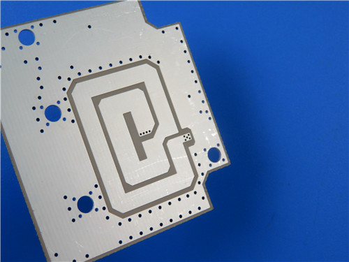
A recent 2-layer RF transceiver board measured 102 mm × 86 mm with 0.7 mm finished thickness. The stackup used 35 μm copper on both layers separated by a 0.635 mm (25 mil) TF960 core. This 1-oz copper weight suits moderate-power RF traces where current capacity and conductor loss both matter.
Design rules included 5/8 mil minimum trace/space and 0.25 mm minimum drill. No blind vias were used, simplifying processing and reducing cost. Via plating was 20 μm, providing reliable barrel conductivity for layer-to-layer signal transitions. Immersion silver finish provided a flat profile and good RF solderability for fine-pitch components. The top side had blue solder mask with white silkscreen; the bottom had neither, typical when it serves as a ground plane. Every board passed 100% electrical test before shipment. This build shows TF960 works within standard 2-layer workflows while delivering the high-frequency performance expected of a premium laminate.
· Microwave/RF Transceivers: Low insertion loss preserves link budget in both transmit and receive chains.
· 5G/6G Massive MIMO Antennas: High Dk enables compact feed networks; low loss keeps efficiency high across large arrays.
· Radar Systems (ADAS, Aerospace): Stable Dk over temperature and low moisture absorption support reliable detection.
· Satellite Communication Payloads: Stable performance under vacuum and thermal cycling.
· High-Power RF Amplifiers: Low Df reduces substrate heat; 1-oz copper supports higher current.
· Test & Measurement Equipment: Tight Dk tolerance supports accurate, repeatable VNA calibrations and fixtures.
While TF960 high frequency PCB is FR4-compatible in processing, several practical points can affect yield and performance in volume production.
1. Drilling. PTFE can smear if feed rates and drill geometry are not optimized. Standard carbide drills with appropriate peck cycles work well.
2. Plating. Through-hole adhesion requires proper surface preparation (etching or plasma treatment). 20 μm plating is a reliable target.
3. Lamination. For multi-layer builds, confirm compatible prepreg and bonding sheets with your fabricator, as not all high-frequency materials bond identically.
4. Impedance Control. With Dk 9.6, 50-ohm traces are narrower than on FR4 for the same thickness. Use the fabricator’s impedance calculator and include test coupons.
Q: How does TF960 compare to RO4350B?
RO4350B has Dk 3.48 and Df 0.0037 at 10 GHz. TF960 offers higher Dk for miniaturization and lower loss, but RO4350B may be preferred when lower Dk is needed for wider, more manufacturable traces. The choice depends on design priorities.
Q: Can TF960 be used in multi-layer boards?
Yes. TF960 cores laminate with compatible prepreg, but confirm specific bonding materials and profiles with your manufacturer. PTFE surfaces require careful preparation for reliable inter-layer adhesion.
Q: Is TF960 more expensive than FR4?
Yes. PTFE-based high-frequency laminates cost significantly more than FR4. The premium is justified where FR4’s higher loss and less stable Dk would degrade system performance. For low-frequency designs, FR4 remains economical.
Q: What assembly temperatures can TF960 withstand?
TF960 supports standard lead-free reflow up to 260°C. Follow normal ESD and moisture handling. Due to different CTE than FR4, pay attention to BGA pad design and solder joint reliability under thermal cycling.
TF960 high DK PCB occupies a specific and valuable niche in high-frequency circuit design. Its Dk of 9.6 enables compact RF layouts, Df of 0.0012 minimizes signal loss, and FR4-compatible processing makes it practical for volume manufacturing. The material is not a universal replacement for FR4—its cost and narrower trace geometries make it unnecessary for low-frequency digital or analog circuits. But for microwave transceivers, radar, satellite communications, and high-power amplifiers, TF960 delivers measurable performance advantages that directly improve system-level metrics such as link budget, energy efficiency, and thermal margin.
Categories
New Blog
Tags
 6-11C Shidai Jingyuan, Fuyong, Baoan, Shenzhen, Guangdong, China 518103


For inquiries about our products or pricelist, please leave to us and we will be in touch within 24 hours.
© Copyright: 2026 Shenzhen Bicheng Electronics Technology Co., Ltd.. All Rights Reserved.

IPv6 network supported


