
 Call Us Now !
Tel : +86 755 27374946
Call Us Now !
Tel : +86 755 27374946
 Order Online Now !
Email : info@bichengpcb.com
Order Online Now !
Email : info@bichengpcb.com
What Makes F4BTD350S PCB the Right Choice for High-Power RF Designs?
What Makes F4BTD350S PCB the Right Choice for High-Power RF Designs?
Quick Answer
The F4BTD350S PCB is a PTFE-based high-frequency circuit board engineered explicitly for high-power radio frequency (RF) and microwave applications where thermal management and signal integrity are non-negotiable. Built on a glass-fiber-reinforced PTFE substrate loaded with high-thermal-conductivity ceramic fillers, it delivers a stable dielectric constant of 3.5 at 10 GHz, an ultra-low dissipation factor of 0.0016, and a thermal conductivity of 1.25 W/m·K—a combination that outperforms standard FR-4 and many mid-tier high-frequency laminates in power-handling capacity and long-term reliability. For engineers designing power amplifiers, antenna feeds, industrial heating systems, or passive components such as couplers and filters, the F4BTD350S substrate reduces insertion loss, improves heat dissipation, and lowers the risk of thermal failure under continuous high-temperature operation.
Key Takeaways
1) Superior thermal performance for power-dense RF:
With 1.25 W/m·K thermal conductivity—roughly three to four times that of conventional FR-4—F4BTD350S PCBs spread heat more evenly across the board, extending component life in power amplifiers and industrial heating equipment.
2) Exceptionally low loss at microwave frequencies:
A dissipation factor of 0.0016 at 10 GHz means less signal energy is converted to heat, preserving output power and reducing thermal load in high-frequency transmit chains.
3) Stable dielectric across temperature and frequency:
Dk of 3.5±0.07 at 10 GHz and a thermal coefficient of Dk of only−45 ppm/°C ensure consistent impedance matching and filter response from−55°C to 150°C.
4) Mechanically robust for manufacturability:
Low CTE in the x/y plane (11/10 ppm/°C) and UL-94 V0 flammability rating improve through-hole reliability, dimensional stability during assembly, and overall safety compliance.
5) Versatile across high-power RF segments:
From base-station power amplifiers and phased-array antennas to RF couplers, power splitters, and industrial microwave heating systems, F4BTD350S covers a wide range of applications where both power handling and low loss matter.
Understanding F4BTD350S: Beyond the Datasheet Numbers
When engineers evaluate high-frequency PCB materials, they often start and end with Dk and Df values. But in high-power RF designs, those two numbers tell only a fraction of the story. What ultimately determines whether a board survives years of continuous operation—and whether it meets regulatory and performance targets—is how the material behaves under combined thermal, electrical, and mechanical stress. This is where F4BTD350S distinguishes itself from commodity PTFE boards and even from some better-known branded alternatives.
Wangling F4BTD350S is a PTFE (polytetrafluoroethylene) resin system reinforced with woven glass fiber and heavily loaded with specialized high-thermal-conductivity ceramic particles. The glass-fiber weave provides mechanical rigidity and dimensional stability, which pure PTFE alone cannot offer. The ceramic filler is the real differentiator: it raises thermal conductivity from the 0.3–0.5 W/m·K range typical of standard PTFE substrates to 1.25 W/m·K. That jump is not incremental—it fundamentally changes how heat generated by power transistors, RF power dividers, or microwave heating elements moves away from the source and into the surrounding structure or heat sink.
For a practical 2-layer F4BTD350S PCB built with 1 oz copper on both sides and a 0.508 mm core, the thermal path from a top-side power device to a bottom-side heat spreader is significantly more efficient than an equivalent FR-4 or standard PTFE board. In power amplifier designs, this translates directly to lower junction temperatures at the same output power, or alternatively, higher achievable output power before derating is required. Field experience from RF manufacturing teams shows that power amplifiers built on high-thermal-conductivity PTFE substrates typically run 15–25°C cooler at the transistor base than comparable units on standard low-loss laminates, depending on power level and airflow.
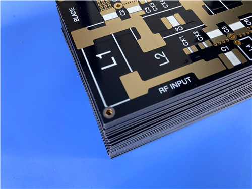
Electrical Performance: Why 0.0016 Dissipation Factor Matters in Practice
Loss in an RF PCB comes from multiple sources—conductor loss, dielectric loss, radiation loss, and leakage. At frequencies above 1 GHz, dielectric loss becomes a significant contributor, and at microwave bands (3–30 GHz), it often dominates the total insertion budget. The dissipation factor (Df) of 0.0016 at 10 GHz places F4BTD350S firmly in the low-loss category, well below the 0.01–0.02 range of FR-4 and even below many mid-range hydrocarbon-ceramic laminates.
Why does this matter beyond the lab bench? In a transmit chain, every decibel lost in the substrate is a decibel that the power amplifier must produce extra—and that extra power turns into heat. Over the lifetime of a base-station amplifier or an industrial microwave generator, those extra watts accumulate into higher energy consumption, more thermal cycling, and shorter component life. For filter and coupler designs, low Df directly translates to sharper roll-off, deeper stop-band rejection, and lower insertion loss in the pass-band, which simplifies system-level tuning and reduces the need for gain compensation stages.
Equally important is dielectric stability. F4BTD350S maintains a Dk of 3.5 with a tolerance of±0.07 across the panel and a thermal coefficient of Dk (TCDk) of−45 ppm/°C from−55°C to 150°C. For precision filters and tightly matched antenna feeds, even a small drift in Dk can shift the center frequency enough to push the design out of specification. The low TCDk of F4BTD350S means that a filter tuned at room temperature will stay within its pass-band window across the full operating temperature range, reducing the need for active compensation or over-design.
Mechanical and Thermal Reliability: The Manufacturing Perspective
One of the less discussed but critical advantages of F4BTD350S is its dimensional stability, driven by a low coefficient of thermal expansion (CTE). In the x-axis, CTE is 11 ppm/°C; in the y-axis, 10 ppm/°C; and in the z-axis, 40 ppm/°C, measured from−55°C to 288°C. The in-plane values are close to that of copper itself (around 17 ppm/°C), which greatly reduces shear stress on copper traces, plated through-holes, and solder joints during thermal cycling.
For PCB fabricators, this has real manufacturing implications. Plated through-holes (PTH) onF4BTD350S boards —even with a finished board thickness of only 0.6 mm and a 20μm copper plating thickness—show consistently higher reliability under thermal shock testing compared to higher-CTE PTFE materials. The glass-fiber reinforcement also improves drillability and reduces smear, resulting in cleaner hole walls and more consistent plating coverage. From a quality-control standpoint, boards built to IPC-Class-2 standards on F4BTD350S routinely pass electrical testing at 100% yield when proper drilling and plating parameters are used.
The material also carries a UL-94 V0 flammability rating and a Comparative Tracking Index (CTI) of 600 V, which simplifies compliance for industrial and telecom end-products. Moisture absorption is≤0.05%, another important parameter for outdoor and high-humidity deployments such as antenna arrays and remote radio units. Low moisture uptake prevents Dk drift, avoids delamination under reflow, and maintains insulation resistance over time—all factors that contribute to long field life with minimal maintenance.
Real-World Applications and Case Experience
F4BTD350S has found its strongest adoption in four application categories, each leveraging a different combination of the material's properties.
1) High-power RF power amplifiers (PAs) are the most common use case. Here, the 1.25 W/m·K thermal conductivity is the primary driver. In L-band and S-band power amplifiers for cellular infrastructure, public safety radio, and radar systems, designers often pair F4BTD350S with thick copper cladding (1 oz or higher) and backside thermal vias to create an efficient heat path from transistor packages to the chassis. Production data from contract manufacturers shows that PA modules on F4BTD350S substrates exhibit lower rates of field returns related to thermal fatigue compared to previous-generation boards using standard PTFE.
2) Antenna feed networks and phased-array elements benefit from the combination of stable Dk, low loss, and low CTE. In array antennas where hundreds or thousands of elements must be phase-matched, board-to-board Dk consistency and temperature stability directly impact beam-pointing accuracy and side-lobe levels. The±0.07 Dk tolerance of F4BTD350S supports tight element-to-element matching without the need for per-board trimming in many designs.
Passive RF components—couplers, filters, and power splitters—are another major segment. For these parts, insertion loss, isolation, and return loss are the key performance metrics, and all three improve when the substrate has low Df and controlled Dk. Manufacturers of directional couplers for test and measurement equipment frequently switch to F4BTD350S when their standard substrate can no longer meet loss targets at higher frequency bands.
3) Industrial heating and microwave processing equipment represent a more specialized but growing application. In these systems, the board itself may carry very high RF power levels and operate in elevated ambient temperatures. The high thermal conductivity, UL-94 V0 rating, and ability to withstand continuous operation at high temperatures make F4BTD350S a natural fit where FR-4 and even some standard PTFE materials would degrade prematurely.
Data Comparison: F4BTD350S Against Common Alternatives
To put F4BTD350S performance in context, it is useful to compare its core parameters against two widely used reference materials: standard FR-4 and a typical mid-range PTFE microwave substrate.
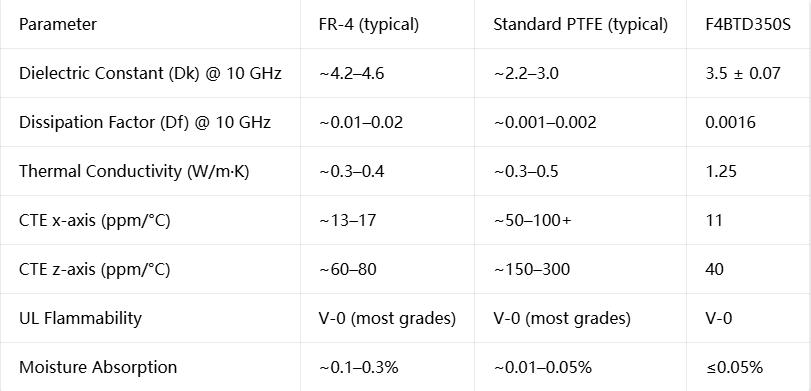
The data shows that F4BTD350S occupies a unique position: it offers the low loss expected from a PTFE-based material while delivering thermal conductivity and in-plane dimensional stability closer to what would normally require a much more expensive specialty ceramic-filled composite. For designs that need both low insertion loss and effective heat dissipation—which is the case for nearly all high-power RF applications—F4BTD350S provides a compelling balance of performance and manufacturability.
Manufacturing Specifications in Context
A representative double-sided F4BTD350S PCB for RF applications might be built with the following parameters, all of which are well within standard fabrication capabilities for experienced high-frequency PCB shops:
These specifications are not extreme or exotic—and that is part of the value proposition. F4BTD350S does not require specialized non-standard processing that would drive up cost or lead time. A competent PCB fabricator experienced with PTFE materials can produce F4BTD350S boards using standard drill bits, plating lines, and lamination cycles, as long as they follow proper PTFE surface preparation for adhesion.
Frequently Asked Questions (FAQ)
Q: Is F4BTD350S suitable for multilayer PCBs, or only 2-layer designs?
A: F4BTD350S is suitable for multilayer and high-layer-count designs, including backplanes. The material's good mechanical properties and dimensional stability support reliable lamination and registration in multilayer stacks. That said, many high-power RF applications that use F4BTD350S are implemented as 2-layer or 4-layer boards because the power devices and transmission lines are often placed on the outer layers for thermal and RF performance reasons.
Q: How does F4BTD350S compare to Rogers RO4000 series materials?
A: Both are ceramic-filled PTFE composites targeting high-frequency applications, and both offer low loss and good thermal performance relative to FR-4. F4BTD350S is positioned as a high-thermal-conductivity option with Dk 3.5 and 1.25 W/m·K thermal conductivity. When selecting between materials, engineers should compare specific grade parameters (Dk, Df, thermal conductivity, CTE), availability, and total cost of fabrication for their specific design rather than relying on brand alone.
Q: Can F4BTD350S PCBs be assembled with standard SMT reflow processes?
A: Yes. F4BTD350S is compatible with standard SMT assembly, including lead-free reflow profiles. Its UL-94 V0 rating, low CTE, and low moisture absorption contribute to reliable soldering and reduce the risk of delamination or pad lifting during reflow. As with any PTFE-based material, proper surface treatment before soldermask and surface-finish application is important for adhesion.
Q: What is the typical lead time for F4BTD350S PCB prototypes?
A: For standard 2-layer F4BTD350S PCBs with common parameters (0.6 mm thickness, 1 oz copper, immersion gold, 0.6 mm minimum hole), prototype lead times are typically in the range of standard high-frequency board fabrication—usually a few weeks depending on panel size, quantity, and testing requirements. Worldwide shipping is available from qualified manufacturers.
Q: Does F4BTD350S meet IPC standards?
A: F4BTD350S PCBs can be manufactured and tested to IPC-Class-2 standards, which is the most common class for commercial and industrial electronic assemblies. Higher classes can be discussed on a case-by-case basis depending on the specific reliability and testing requirements of the end application.
Closing Thoughts
Selecting the right substrate for a high-power RF design is always a trade-off between electrical performance, thermal management, mechanical reliability, and cost. F4BTD350S stands out because it addresses the thermal bottleneck that plagues so many power-amplifier and industrial-microwave designs—without sacrificing the low-loss and stable-dielectric properties expected from a premium PTFE material. For engineers who have been pushing standard PTFE or FR-4 boards to their thermal limits, migrating to F4BTD350S often yields measurable improvements in operating temperature, component longevity, and overall system reliability. As with any material change, validating with a prototype build and thermal characterization under real operating conditions is always recommended—but for a growing number of high-power RF applications, F4BTD350S has become the default starting point rather than an exotic upgrade.
Categories
New Blog
Tags
 6-11C Shidai Jingyuan, Fuyong, Baoan, Shenzhen, Guangdong, China 518103


For inquiries about our products or pricelist, please leave to us and we will be in touch within 24 hours.
© Copyright: 2026 Shenzhen Bicheng Electronics Technology Co., Ltd.. All Rights Reserved.

IPv6 network supported


