
 Call Us Now !
Tel : +86 755 27374946
Call Us Now !
Tel : +86 755 27374946
 Order Online Now !
Email : info@bichengpcb.com
Order Online Now !
Email : info@bichengpcb.com
How Does RT/duroid 6010.2LM’s High Dk Enable Circuit Miniaturization in 4-Layer PCBs?
How Does RT/duroid 6010.2LM’s High Dk Enable Circuit Miniaturization in 4-Layer PCBs?
In the world of high-frequency RF and microwave engineering, the mantra is often "smaller, faster, cheaper." However, achieving miniaturization without compromising signal integrity is a significant challenge. As operating frequencies push into the X-band and beyond, the physical dimensions of passive structures—transmission lines, impedance matching networks, and antennas—become critically small.
For designers and procurement specialists looking for a competitive edge, the choice of laminate material is the deciding factor. RT/duroid 6010.2LM by Rogers Corporation is a cornerstone material for size reduction. But how exactly does its high dielectric constant (Dk) facilitate miniaturization in a complex 4-layer PCB?
As a supplier specializing in precise, high-frequency PCB fabrication, we regularly manufacture boards utilizing this specific material. Let’s break down the physics and the practical application, using a recent 4-layer project as a case study.
The Physics of Miniaturization: Wavelength and Dk
To understand miniaturization, we look at the wavelength of a signal traveling through a medium. The guided wavelength (λ) is inversely proportional to the square root of the effective dielectric constant (Dk) of the substrate.
λ=λ₀/√Dk
Whereλ₀is the wavelength in a vacuum. In simple terms: the higher the Dk, the shorter the wavelength. Shorter wavelengths mean that resonant structures—like patch antennas or impedance transformers—can be physically smaller while maintaining the same electrical length (e.g.,λ/4 orλ/2).
RT/duroid 6010.2LM boasts a dielectric constant of 10.2 +/- 0.25. This is significantly higher than standard FR-4 (typically 4.5) or even standard RF materials like RT/duroid 5880 (Dk 2.2). By embedding circuits in a material with a Dk of 10.2, engineers can shrink the physical footprint of their circuits by approximately 40-60% compared to lower Dk alternatives.
Beyond the Material: A 4-Layer Miniaturization Case Study
While theory is compelling, real-world application requires precise engineering. High Dk PCB materials are notoriously difficult to process due to their ceramic content, which makes them brittle. Furthermore, integrating them into a multilayer stackup requires careful thermal mechanical management.
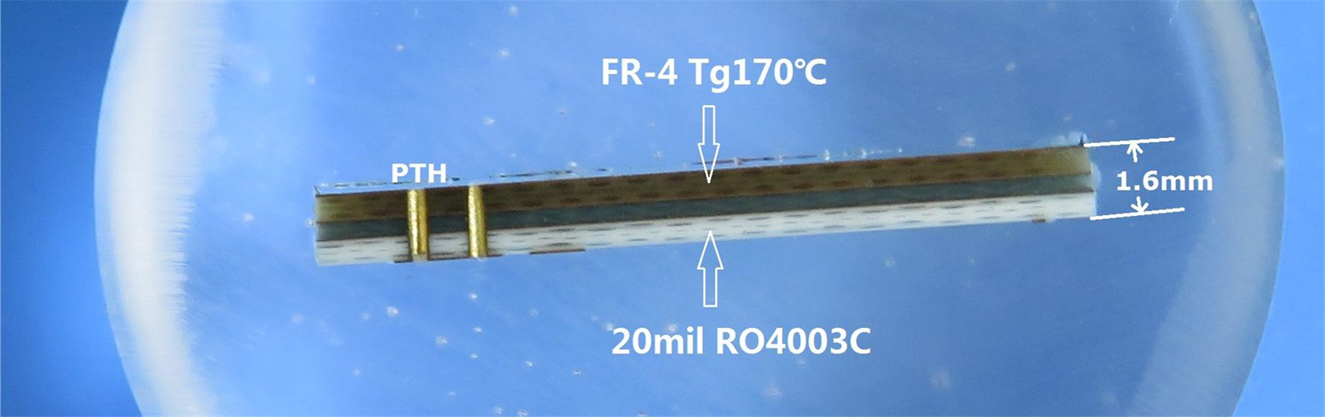
Consider the specifications of a recent 4-layer board we manufactured:
Stackup:
This stackup illustrates exactly how miniaturization is achieved in a practical sense.
1. The "Thick Copper Sandwich" for Power and Ground
The 1.27mm (50mil) cores provide a robust dielectric between Layer 1 and Layer 2, and Layer 3 and Layer 4. Because the Dk is so high, the 50mil thickness does not negatively impact the trace width requirements for 50-ohm lines. In fact, it allows for wider, more forgiving traces on the outer layers than a thinner, lower Dk material would require. This improves yield during manufacturing while keeping the board surface compact.
2. CTE Matching for Reliability
One of the hidden enablers of miniaturization is reliability. As components get smaller, the mechanical stress on vias and plated through-holes increases.
The RT/duroid 6010.2LM material features a Coefficient of Thermal Expansion (CTE) matched to copper (24 ppm/°C in the X and Y axes). In a 4-layer board with 28 vias and 16 thru-hole pads, this is critical. If the material expanded significantly more than the copper plating (20μm via plating thickness) during thermal cycling, the vias would crack, killing the miniature circuit. The matched CTE ensures that the "miniature" board survives real-world conditions.

The Design Advantages of High Dk in Multilayer RF Boards
Our specific PCB data sheet highlights several points that are direct benefits of using Rogers 6010.2LM in a miniaturized format:
Tight Dk Control for Impedance Accuracy: The specification of Dk 10.2 +/- 0.25 is extremely tight. For the designer, this means that the simulated impedance of a 5/7 mil trace will match the actual impedance of the fabricated board. This consistency allows designers to push the limits of trace spacing without fear of impedance mismatch, which is vital for the 21 high-frequency components mounted on this board.
Low Loss at High Frequency: Miniaturization is useless if the signal is attenuated. With a dissipation factor of 0.0023 at 10 GHz, the 6010.2LM ensures that while the circuit geometry shrinks, the signal strength remains robust. This makes it ideal for the "Typical Applications" listed, such as Satellite Communications and Aircraft Collision Avoidance Systems, where every dB of signal strength matters.
Simplified Fabrication: The product features specify "Reliable plated through-holes in multi-layer boards." For this 4-layer design, we utilized standard thru-hole vias rather than expensive blind vias (as noted: "No Blind vias"). The material's stability allows us to drill and plate the 0.5mm holes without the resin smear or barrel cracking often seen with softer materials. This keeps the manufacturing cost-effective while maintaining the IPC-Class-2 quality standard required for the application.
Thermal Management in a Small Package
One of the trade-offs of miniaturization is heat density. When you shrink the board, the heat generated by power amplifiers has less surface area to spread across.
RT/duroid 6010.2LM addresses this with a thermal conductivity of 0.86 W/mK. While this might not seem high compared to aluminum-backed substrates, it is excellent for a ceramic-PTFE composite. Combined with the finished copper weight of 1oz (1.4 mils) on the outer layers, the board can effectively wick heat away from active components and into the ground planes (Layer 2) or heat sinks attached to the ENIG-finished pads.
Conclusion: Size Reduction Without Compromise
RT/duroid 6010.2LM is more than just a high Dk material; it is an enabler of modern RF system architecture. By allowing the physical length of a wave to shrink, it allows engineers to pack more functionality—like Patch Antennas and Power Amplifiers—into a smaller volume.
In a 4-layer configuration, the material provides the mechanical stability to support a thick board (2.8mm) with a dense via field (28 vias) and tight trace geometries (5/7 mils). It bridges the gap between the need for extreme electrical performance and the practical demand for durable, manufacturable hardware.
As a supplier, our role is to take your Gerber RS-274-X files and the promise of this material and turn it into a reality. With 100% electrical testing and strict adherence to the Rogers processing guidelines, we ensure that the miniaturization you designed on screen performs perfectly in the field.
Categories
New Blog
Tags
 6-11C Shidai Jingyuan, Fuyong, Baoan, Shenzhen, Guangdong, China 518103


For inquiries about our products or pricelist, please leave to us and we will be in touch within 24 hours.
© Copyright: 2026 Shenzhen Bicheng Electronics Technology Co., Ltd.. All Rights Reserved.

IPv6 network supported


