How to choose PCB substrate?
In recent years, the printed circuit board market has shifted from traditional hardware products such as desktop computers to wireless communications such as servers and mobile terminals. The mobile communication equipment represented by smart phone promotes PCB to develop towards high-density, lightweight and multi-function. Printed circuit technology cannot be implemented without substrate materials whose technical requirements are closely related to the performance of the PCB. Therefore, the choice of substrate material plays a crucial role in improving the quality and reliability of PCB and its final product.
Meet the requirements of high density and fine line
Requirements for copper foil
All PCBS are moving toward higher density and thinner lines, especially HDI PCBS (
High density Interconnect PCBS). Ten years ago, HDI PCBS were defined by IPC as PCBS with line width (L) and line spacing (S) of 0.1mm or less. However, at present, the standard values of L and S in the current electronics industry can be as low as 60μm, and under advanced conditions, the values can be as low as 40μm.
Traditional circuit pattern formation methods involve imaging and etching processes that result in minimum L and S values of 30μm using thin copper foil substrates in the thickness range of 9μm to 12μm.
Due to the high cost, stacking, and defect of CCL, many PCB manufacturers prefer to use etching and reducing copper foil instead of copper foil of 18μm thickness. This method is not actually recommended because it involves too much process and the thickness is difficult to control, resulting in higher cost. As a result, thinner copper foil is better. In addition, standard copper foils do not work when the L and S values of the plates are less than 20μm. Finally, it is recommended to use ultra-thin copper foil, as the copper thickness should be controlled in the range of 3μm to 5μm.
In addition to the thickness of copper foil, current fine circuits also require a low-roughness copper foil surface. In order to improve the bonding ability between copper foil and matrix material and ensure the stripping strength of conductor, the copper foil plane was coarsely treated, and the roughness of ordinary copper foil was greater than 5μm.
In order to improve the peel strength of copper foil, the ridges are embedded into the substrate material. However, the attempt to control lead accuracy away from excessive etching during circuit etching tends to cause hump contamination, which may lead to short-circuiting or reduced insulation capacity between wires, particularly affecting fine circuits. Therefore, copper foil with low roughness (less than 3μm or even 1.5μm) is required.
Although the roughness of the copper foil is reduced, it is still necessary to maintain the stripping strength of the conductor, which will cause special surface forming on the surface of the copper foil and the substrate material, which will help ensure the stripping strength of the conductor.
Requirements for insulating dielectric laminates
One of the main technical characteristics of an HDI PCB is the build process. The commonly used lamination of RCC (resin-coated copper) or prepreg epoxy glass cloth and copper foil rarely results in fine circuits. SAP and MSPA are preferred, which means that an insulating dielectric film is pressed together with an electroless copper plating layer to produce a copper conducting plane. Due to the thin copper plane, fine circuits can be produced.
One of the key points of SAP is the layered piezoelectric dielectric material. In order to meet the requirements of high-density fine circuits, a number of requirements must be placed on laminated materials, including dielectric properties, insulation, heat resistance and adhesion, as well as technical adaptability to HDI PCB compatibility.
In the global semiconductor packaging, IC packaging substrate has been converted from ceramic substrate to organic substrate. The pitch of FC encapsulated substrates is getting smaller and smaller, so the current typical values of L and S are 15μm and will be smaller.
Multilayer substrate performance should emphasize low dielectric properties, low coefficient of thermal expansion (CTE), and high heat resistance, which refers to low-cost substrates that meet performance objectives. Today, MSPA technology is used to combine layers of insulating dielectric with thin copper foil through the mass production of fine circuits. SAP is used to manufacture circuit patterns with L and S values less than 10μm.
The high density and thinness of the PCB causes the HDI PCB to change from laminate with a core to any layer without a core. For an HDI PCB with the same function, the area and thickness of the PCB with interconnect capability at any layer is 25% less than that of the PCB with core layer. Both HDI PCBS must use a thinner dielectric layer with better electrical properties.
Demand for high frequency and high speed
Electronic communication technology has developed from wired to wireless, from low frequency to high frequency. The performance of smartphones has been upgraded from 4G to 5G, requiring faster transmission speeds and more data.
The arrival of the global cloud computing era leads to the double growth of data flow, and the trend of high frequency and high speed of communication equipment is obvious. In order to meet the requirements of high frequency and high speed transmission, high-performance materials are the most important elements, in addition to reducing signal interference and consumption, signal integrity and manufacture compatible with the design requirements in PCB design.
The engineer's main job is to improve PCB speed and deal with signal integrity problems by relying on the properties of electrical signal loss. Based on more than ten years of PCB manufacturer manufacturing service, as a key factor influencing substrate material selection, it is considered as intermediate Dk/Df laminates when the dielectric constant (Dk) is less than 4 and the dielectric loss (Df) is less than 0.010, and as low Dk/Df laminates when the Dk is less than 3.7 and Df is less than 0.005. Currently, many types of substrate materials are available on the market.
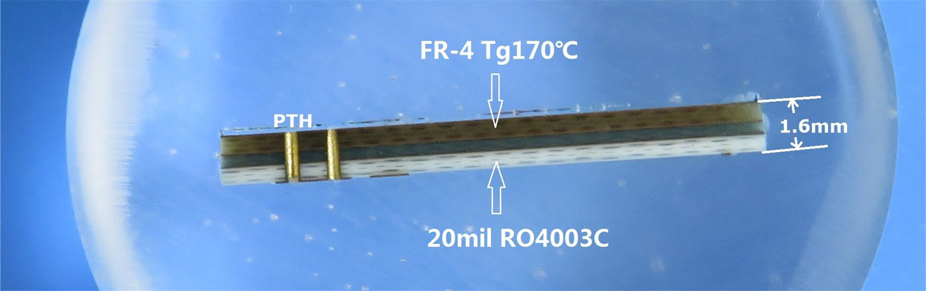
So far, the commonly used hf circuit board substrate materials are mainly the following three: fluorinated resin, PPO or PPE resin and modified epoxy resin. Fluorine series dielectric substrates with the lowest dielectric properties (e.g. PTFE) are commonly used in products with frequencies of 5GHz or higher. Modified epoxy FR-4 or PPO substrates are suitable for products with frequencies in the 1GHz to 10GHz range.
Comparing these three types of hf substrate materials, epoxy resin has the lowest price, while fluorine series resin has the highest price. In terms of dielectric constant, dielectric loss, water absorption and frequency characteristics, fluorine resin performs best, while epoxy resin performs poorly. When the product is applied at frequencies higher than 10GHz, only fluorine series resins work. Disadvantages of PTFE include high cost, poor rigidity and high coefficient of thermal expansion.
For PTFE, bulk inorganic materials such as silica can be used as filler material or glass cloth to enhance the rigidity of the substrate and reduce the coefficient of thermal expansion. In addition, due to the inert nature of the polyfluoroethylene molecule, it is difficult for the polyfluoroethylene molecule to combine with copper foil, so it is necessary to achieve a special surface molding compatible with copper foil. The treatment involves chemically etching the surface of polyethylene to increase surface roughness or adding adhesive films to increase adhesion. With the application of this method, dielectric properties may be affected, and further development of the entire fluorine series hf circuit must be carried out.
Unique insulating resins consisting of modified epoxy resins or PPE with TMA, MDI and BMI combined with glass cloth have found more applications. Similar to FR-4 CCL, it also has excellent heat and dielectric properties, mechanical strength, and PCB manufacturability, all of which make it more desirable than PTFE-type substrates.
In addition to the performance requirements of insulating materials such as resin, the surface roughness of copper as a conductor is also an important factor affecting signal transmission loss, which is the result of skin effect. In short, the skin effect is that the electromagnetic induction and inductance generated by the wire in high-frequency signal transmission becomes so concentrated in the center of the wire's cross-sectional area that the driving current or signal concentrates on the wire's surface. The surface roughness of the conductor plays a key role in affecting the transmission signal loss.
At the same frequency, the high surface roughness of copper leads to high signal loss. Therefore, the surface roughness of copper must be controlled in actual manufacturing and should be kept as low as possible without affecting the adhesion. Special attention must be paid to signals in the 10 GHz or higher frequency range. The roughness of copper foil should be less than 1μm, and 0.04μm of supersurface copper foil is the best. The surface roughness of copper foil must be combined with appropriate oxidation treatment and bonding resin system. In the near future, there may be a copper foil shape that is not coated with resin, and it has higher peel strength and does not affect dielectric loss.
High heat resistance and heat dissipation requirements
With the development trend of miniaturization and high function, electronic equipment tends to generate a large amount of heat, so the thermal management of electronic equipment requires higher and higher requirements. One way to solve this problem is the research and development of thermal conductive PCB. PCB heat resistance and good heat dissipation of the main condition is the substrate heat resistance and heat dissipation. Current improvements in PCB thermal conductivity are made through the addition of resins and fillers, but only in limited categories. The typical method is to use IMS or metal core PCBS that act as heating components. Compared with traditional radiators and fans, this method has the advantages of small size and low cost.
Aluminum is a very attractive material, with the advantages of abundant resources, low cost, excellent thermal conductivity and strength. In addition, it is very environmentally friendly and can be used on most metal substrates or metal cores. Because of the advantages of economy, reliable electrical connections, thermal conductivity and high strength, solderless and lead-free,
aluminum-based circuit boards have been used in consumer products, automotive, military and aerospace products. There is no doubt that the heat resistance and heat dissipation of the metal substrate is the key, the key lies in the adhesion between the metal plate and the circuit board.
How to determine PCB substrate material?
In the modern electronic age, the miniaturization and thinness of electronic equipment make it necessary to have rigid PCB and flexible/rigid PCB. So what type of substrate material is suitable for them?
The number and performance of rigid and flexible/rigid PCBS are increasing. For example, polyimide films can be classified into several categories, including transparent, white, black and yellow with high heat resistance and low thermal expansion coefficient, in order to be applied to different situations. Similarly, cost-effective polyester film substrates have been accepted by the market due to their high elasticity, dimensional stability, film surface quality, photoelectric coupling and environmental resistance to meet the changing needs of users.
Similar to rigid HDI PCB, flexible PCB must adapt to the requirements of high speed and high frequency signal transmission, and the dielectric constant and dielectric loss of flexible substrate materials must also be concerned. Flexible circuits can be composed of polytetrafluoroethylene and advanced polyimide substrates. Inorganic dust and carbon fiber can be added to the polyimide resin to produce three layers of flexible thermal conductive substrates. The inorganic filling material may be aluminum nitride, alumina or hexagonal boron nitride. This type of substrate material has a thermal conductivity of 1.51W/mK and is able to resist a voltage of 2.5kV and a curvature of 180 degrees.
Flexible PCB is mainly used in smart phones, wearable devices, medical devices and robotics, which puts forward new requirements for flexible PCB structure. To date, some new products have been developed that contain flexible PCBS, such as ultra-thin flexible multi-layer PCBS, whose thickness has been reduced from 0.4mm to 0.2mm. By using polyimide substrate materials with low Dk and Df, high-speed transmission flexible PCBS can reach transmission speeds of up to 5Gbps. High-power flexible PCB adopts conductors with thickness greater than 100μm to meet the requirements of high-power and high-current circuits. All of these special flexible PCBS naturally acquire unconventional substrate materials.

 Call Us Now !
Tel : +86 755 27374946
Call Us Now !
Tel : +86 755 27374946
 Order Online Now !
Email : info@bichengpcb.com
Order Online Now !
Email : info@bichengpcb.com
 6-11C Shidai Jingyuan, Fuyong, Baoan, Shenzhen, Guangdong, China 518103


