

 Call Us Now !
Tel : +86 755 27374946
Call Us Now !
Tel : +86 755 27374946
 Order Online Now !
Email : info@bichengpcb.com
Order Online Now !
Email : info@bichengpcb.com

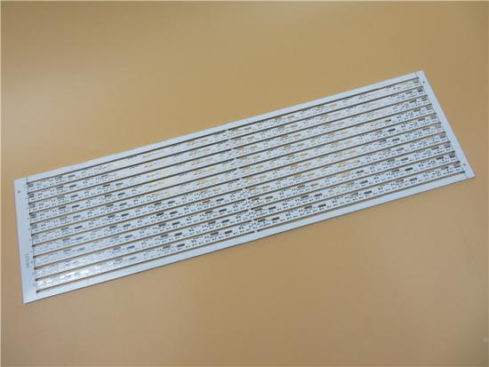
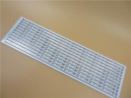
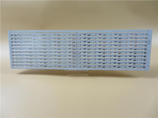
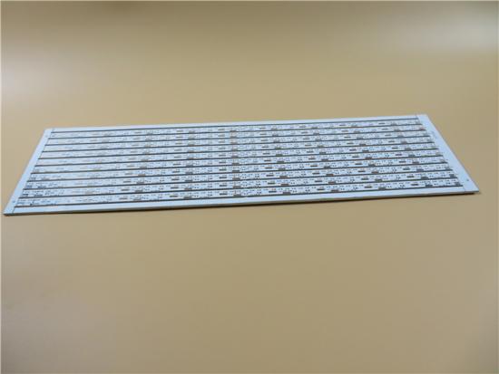
This is a type of double sided aluminum based PCB
for the application of switch regulator.
Item NO.:
BIC-751-v42.0Order(MOQ):
1-10Payment:
T/TProduct Origin:
ChinaShipping Port:
ShenzhenLead Time:
7-10 daysDouble Sided Aluminum PCB Dual Layer Aluminum Circuit Board 2-Layer MCPCB
(Aluminum PCB’s are custom-made products, the picture and parameters shown are just for reference)
1.1 General Description:
This overall thickness is 2.0mm typical from copper to aluminum base, >2000V AC isolation, 1 W/MK thermal conductivity, 2oz copper each layer. The CCL plate is from Totking, ink of solder mask and silkscreen from Taiyo. It's fabricated per IPC 6012 Class 2 using supplied Gerber data. 25 boards are packed for shipment.

1.2 PCB Specifications:
| PCB SIZE | 500 x 150mm=10PCS |
| BOARD TYPE | IMS mcpcb |
| Number of Layers | Double sided PCB, Metal core PCB |
| Surface Mount Components | YES |
| Through Hole Components | NO |
| LAYER STACKUP | copper ------- 70um(2oz) |
| dielectric material 75um | |
| copper ------- 70um(2oz) | |
| dielectric material 75um | |
| Aluminum backed 1.8mm | |
| TECHNOLOGY | |
| Minimum Trace and Space: | 5.98mil/6.18mil |
| Minimum / Maximum Holes: | 0.3/2.2mm |
| Number of Different Holes: | 5 |
| Number of Drill Holes: | 548 |
| Number of Milled Slots: | 11 |
| Number of Internal Cutouts: | 0 |
| Impedance Control | no |
| BOARD MATERIAL | |
| Thermal conductivity | 2W / MK |
| Final foil external: | 2oz |
| Final foil internal: | 2oz |
| Final height of PCB: | 2.1mm ±0.2 |
| PLATING AND COATING | |
| Surface Finish | Hot Air Soldering Leveling(HASL),lead free, Sn>=2.54µm |
| Solder Mask Apply To: | Top, 12micon Minimum. |
| Solder Mask Color: | Super White for LED |
| Solder Mask Type: | LPSM |
| CONTOUR/CUTTING | Routing |
| MARKING | |
| Side of Component Legend | TOP |
| Colour of Component Legend | Black |
| Manufacturer Name or Logo: | Marked on the board in a conductor and leged FREE AREA |
| VIA | via tented. |
| FLAMIBILITY RATING | UL 94-V0 Approval MIN. |
| DIMENSION TOLERANCE | |
| Outline dimension: | 0.0059" (0.15mm) |
| Board plating: | 0.0030" (0.076mm) |
| Drill tolerance: | 0.002" (0.05mm) |
| TEST | 100% Electrical Test prior shipment |
| TYPE OF ARTWORK TO BE SUPPLIED | email file, Gerber RS-274-X, PCBDOC etc |
| SERVICE AREA | Worldwide, Globally. |
1.3 Applications of Aluminum PCB:
Power Hybrid IC
Audio Frequency Apparatus:
Input / Output Amplifier, Balanced Amplifier, Pre-amplifier, Audio amplifier
Power supply device: Switch regulator, DC/AC Converter, Switch regulator
Communication electronic equipment: High frequency generator, Filter appliance, Transmission circuit
Office automation equipment: Motor drive
Automotive: Electronic regulator, Igniter, Power controller
Computer: CPU board, Floppy disk drive, Power supply unit
Power module: Converter, Solid relay, Rectifier bridge
Lamp lighting: All kinds of energy-saving and gorgeous LED lights

1.4 Layer up:
The most common MCPCB construction consists of the following 3 layers:
1) A metal substrate, typically aluminum. In some applications, a copper substrate is more appropriate due to its high thermal conductivity than aluminum (401W/MK versus 237 W/MK) but more expensive.
2) Epoxy dielectric layer. This is the most important layer in the MCPCB construction as it affects the thermal performance, electrical breakdown strength, and, in some cases, the solder joint performance of the MCPCB system. The typical thermal conductivity of the dielectric layer on a MCPCB is 1W/MK. A higher value is better for good thermal performance. A thinner dielectric layer is better for thermal performance as well but can negatively impact the ability of the MCPCB to withstand a high potential test to meet minimum electrical safety standards as required in certain lighting markets. The typical dielectric thickness layer is 100μm.
3)Top copper layer. A thicker copper layer improves heat spreading into the PCB but may pose challenges for PCB manufacturers when fabricating narrow traces or spaces. A copper thickness of 1oz (35μm) or 2oz (70μm) is common.
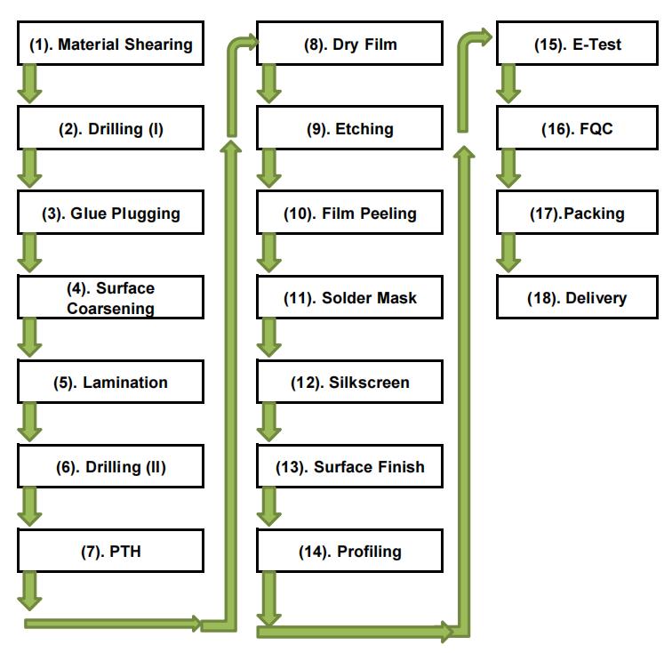
1.5 Manufacturing Process of MCPCB:
The process can be described as a flow diagram as follows.
1.6 Metal Core PCB Capability 2022:
| NO. | Parameter | Value |
| 1 | Type of Metal Core | Aluminum, Copper, Iron |
| 2 | Model of Metal Core | A1100, A5052, A6061, A6063, C1100 |
| 3 | Surface Finish | HASL, Immersion Gold, Immersion Silver, OSP |
| 4 | Thickness of Surface plating | HASL: Sn>2.54µm, ENIG: Au 0.025-0.1µm, Ni 2.5-5µm |
| 5 | Layer Count | 1-2 Layers |
| 6 | Maximum of Board Size | 23" x 46" (584mm×1168mm) |
| 7 | Mininum of Board Size | 0.1969" x 0.1969" (5mm×5mm) |
| 8 | Board Thickness | 0.0157" x 0.2362" (0.4-6.0mm) |
| 9 | Copper Thickness | 0.5OZ(17.5µm),1OZ(35µm),2OZ(70µm),3OZ(105µm),4OZ(140µm) to 10oz (350µm) |
| 10 | Minimum Track Width | 5mil (0.127mm) |
| 11 | Minimum Space | 5mil (0.127mm) |
| 12 | Minimum Hole Size | 0.0197" (0.5mm) |
| 13 | Maximum Hole Size | No limit |
| 14 | Minimum Holes Punched | PCB thickness <1.0mm: 0.0394" (1.0mm) |
| PCB thikness 1.2-3.0mm: 0.0591" (1.5mm) | ||
| 15 | PTH Wall Thickness | >20µm |
| 16 | Tolerance of PTH | ±0.00295" (0.075mm) |
| 17 | Tolerance of NPTH | ±0.00197" (0.05mm) |
| 18 | Deviation of Hole Position | ±0.00394" (0.10mm) |
| 19 | Outline Tolerance | Routing: ±0.00394" (0.1mm) |
| Punching: ±0.00591" (0.15mm) | ||
| 20 | Angle of V-cut | 30°, 45°, 60° |
| 21 | V-cut Size | 0.1969" x 47.24" (5mm×1200mm) |
| 22 | Thickness of V-cut Board | 0.0236" x 0.1181" (0.6-3mm) |
| 23 | Tolerance of V-cut Angle | ±5º |
| 24 | V-CUT Verticality | ≤0.0059" (0.15mm) |
| 25 | Minimum Square Slots Punched | PCB thickness < 1.0mm: 0.0315" x 0.0315" (0.8 x 0.8mm) |
| PCB thickness 1.2-3.0mm: 0.0394" x 0.0394" (1.0 x 1.0mm) | ||
| 26 | Minimum BGA PAD | 0.01378" (0.35mm) |
| 27 | Minimum Width of Solder Mask Bridge. | 8mil (0.2032mm) |
| 28 | Minimum Thickness of Solder Mask | >13µm (0.013mm) |
| 29 | Insulation Resistance | 1012ΩNormal |
| 30 | Peel-off Strength | 2.2N/mm |
| 31 | Solder float | 260℃3min |
| 32 | E-test Voltage | 50-250V |
| 33 | Thermal Conductivity | 0.8-8W/M.K |
| 34 | Warp or Twist | ≤0.5% |
| 35 | Flammability | FV-0 |
| 36 | Minimum Height of Component indicator | 0.0059"(0.15mm) |
| 37 | Minimum Open Solder Mask on Pad | 0.000394" (0.01mm) |
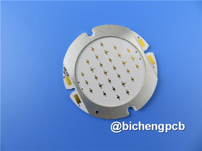
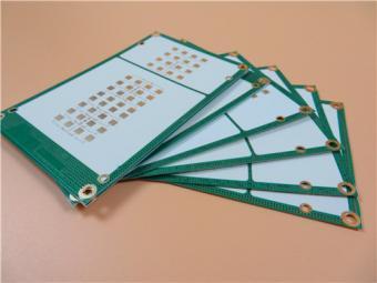
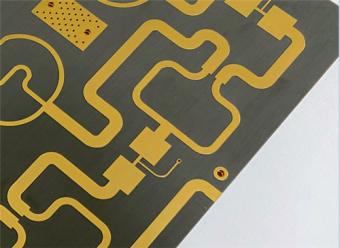
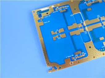
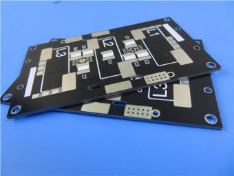
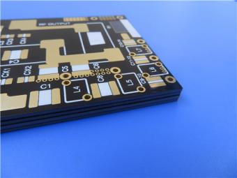
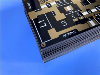
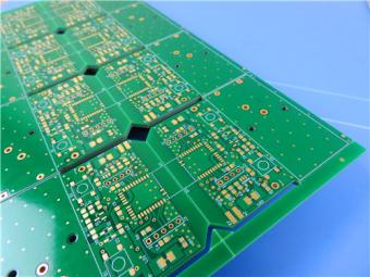
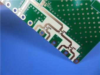
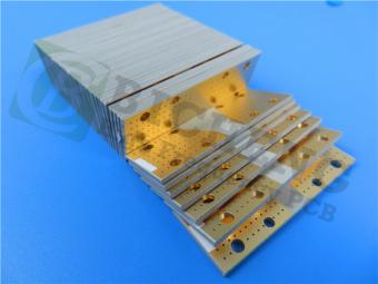
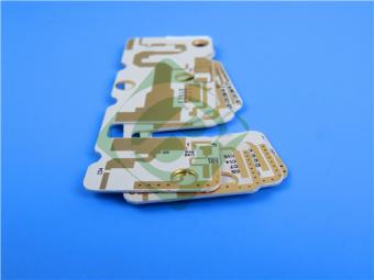
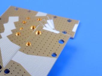
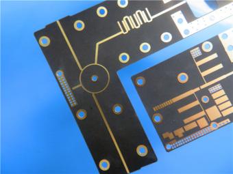
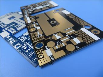
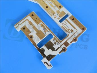
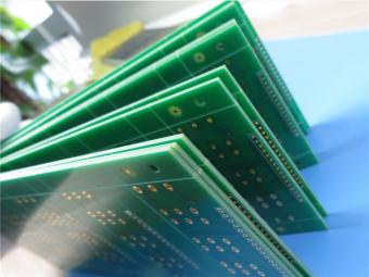
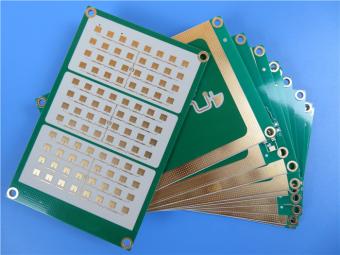
1.7 More Displays of Double Sided Aluminum PCB:

")
")
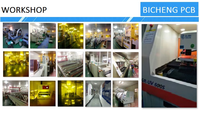
BICHENG PCB WORKSHOP:
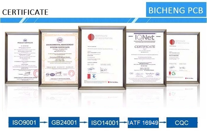
BICHENG PCB CERTIFICATE:
BICHENG MAIN COURIERS:

If you have questions or suggestions,please leave us a message,we will reply you as soon as we can!
Categories
New Products
Wangling 5mil 0.127mm TFA300 Core 2-layer Immersion Gold Green Solder Mask PCB
7.5mil AGC Taconic TLY-5 Substrate Custom PCB EPIG Finish Bare Copper
10mil Rogers CuClad 250 Immersion Gold 2-Layer Rigid Microwave PCB
20mil F4BTMS450 Wangling DK4.5 Laminate Custom PCB HASL LF Finsh
F4BME275 Wangling DK2.75 Laminate 2-Layer 1.6mm Pure Gold RF Custom PCB
Wangling F4BTD350S High Frequency PCB 2-layer 20mil Thick ENIG DK3.5 Substrate
12-layer TG200 TU-872 SLK High-Speed FR4 1.68mm PCB with ENIG Impedance Control
12-Layer RO4350B + RO3010 3.14mm Hybrid PCB Nickel-Free EPIG Surface Finish Blind Via
Rogers RO3010 high frequency circuit laminates are designed for commercial microwave and radio frequency applications.
The RO3006 2-layer 10mil PCB is a high-reliabilityRF circuit board designed for demanding microwave applications.
Whether you’re designing compact RF devices or mission-critical aerospace systems, our RF-10 25mil substrate PCB delivers the performance, reliability, and cost-efficiency you need.
Rogers' TMM 13i thermoset microwave laminates are ceramic, hydrocarbon, thermoset polymer composites designed for high PTH reliability stripline and microstrip applications. It has the dielectric constant of 12.85 and dissipation factor of 0.0019
The RF-60TC PCB 5mil is a cutting-edge, high-performance printed circuit board specifically designed for high-power RF and microwave applications.
Rogers Diclad 527 laminates offer a higher proportion of fiberglass reinforcement compared to PTFE content.
S1000-2M is a type of High Tg printed circuit board material manufactured by Shengyi with characteristics of high performance and low CTE.
The hybrid PCB can be a mixture of FR-4 and high frequency material, and a mixture of high frequency material with different dielectric constant (DK)
 6-11C Shidai Jingyuan, Fuyong, Baoan, Shenzhen, Guangdong, China 518103


For inquiries about our products or pricelist, please leave to us and we will be in touch within 24 hours.
© Copyright: 2026 Shenzhen Bicheng Electronics Technology Co., Ltd.. All Rights Reserved.

IPv6 network supported


