Seeking a High-Performance, Reliable HF PCB Material? What Can F4BTM Offer Your Design?
In the rapidly advancing world of wireless technology, the demand for high-frequency printed circuit boards (PCBs) that offer exceptional electrical performance, unwavering reliability, and cost-effectiveness is greater than ever. Wangling F4BTM High Frequency PCB emerges as a premier solution engineered to meet these rigorous challenges head-on. This article delves into the unique composition, outstanding features, and extensive capabilities of F4BTM, illustrating why it is the material of choice for cutting-edge applications.
Advanced Material Composition: The Foundation of Excellence
The superior performance of Wangling F4BTM series laminates originates from its sophisticated material science. The base structure is composed of a robust fiberglass cloth reinforced with a proprietary blend of nano-ceramic fillers and Polytetrafluoroethylene (PTFE) resin. This combination is subjected to strictly controlled pressing processes to ensure consistency and quality. Building upon the proven F4BM dielectric layer foundation, the strategic incorporation of high-dielectric, low-loss nano-ceramic particles yields a composite material with significantly enhanced properties. The result is a laminate that exhibits a higher and more stable dielectric constant (Dk), superior heat resistance, a reduced coefficient of thermal expansion (CTE), elevated insulation resistance, and improved thermal conductivity, all while meticulously preserving the low-loss characteristics critical for high-frequency signal integrity.
Furthermore, the F4BTM PCB series offers versatility through its copper foil options. The standard F4BTM variant is paired with Electrodeposited (ED) copper foil, providing a reliable and cost-effective solution. For applications where performance is paramount, the F4BTME variant utilizes Reverse-Treated Foil (RTF). This choice delivers exceptional Passive Intermodulation (PIM) performance, enables more precise control over fine lines during etching, and contributes to lower overall conductor loss, making it ideal for sensitive RF systems.
Comprehensive Feature Set for Superior Design Flexibility

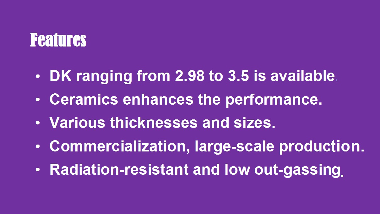
F4BTM PCB is distinguished by a wide array of features that provide engineers with remarkable design flexibility. Its stable Dielectric Constant (Dk) can be tailored within a range of 2.98 to 3.5, allowing for precise impedance matching and optimized circuit design for specific frequency bands. The nano-ceramic enhancement is pivotal, boosting the material's overall performance to suit the most demanding high-frequency and high-speed digital applications.
This high-performance material is available in a diverse selection of standard thicknesses and panel sizes, accommodating a broad spectrum of project requirements without necessitating custom orders, which translates into significant cost savings. Its formulation is designed for excellent manufacturability, supporting large-scale production runs with high yield, thereby establishing F4BTM as a highly cost-effective choice without compromising on quality. Additionally, F4BTM laminates possess radiation-resistant and low out-gassing properties, guaranteeing long-term reliability and functionality even in the harsh environments of aerospace and satellite applications.
Extensive PCB Manufacturing Capabilities

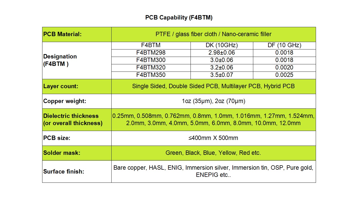
To fully leverage the advantages of F4BTM material, Wangling supports it with a comprehensive suite of advanced PCB manufacturing capabilities. We possess the expertise to produce a wide variety of board configurations, including single-sided, double-sided, complex multilayer, and hybrid PCBs that combine different materials.
We offer flexibility in copper weight, with standard options of 1oz (35µm) and 2oz (70µm), to meet varying current-carrying and conductivity requirements. For dielectric and overall board thickness, we provide an extensive selection ranging from a thin 0.25mm up to a substantial 12.0mm, catering to diverse mechanical and electrical design specifications. Our manufacturing lines can accommodate PCBs with maximum dimensions of 400mm x 500mm.
To support both functional and aesthetic needs, we offer solder mask in various colors, including green, black, blue, yellow, and red. For surface finish, we support all common and advanced types such as bare copper, HASL (Hot Air Solder Leveling), ENIG (Electroless Nickel Immersion Gold), immersion silver, immersion tin, OSP (Organic Solderability Preservative), pure gold, and ENEPIG (Electroless Nickel Electroless Palladium Immersion Gold).

Diverse Application Spectrum
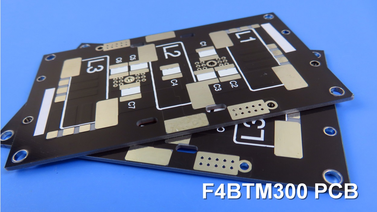
A prime example of F4BTM PCB in use is a circuit board designed with a DK of 3.0, constructed on a 1.524mm thick substrate and finished with HASL. The applicability of DK 3.0 F4BTM PCB is vast, covering critical sectors such as:
Antenna systems (including base station antennas)
Mobile Internet infrastructure
Sensor Networks and IoT devices
Radar and Millimeter Wave Radar systems
Aerospace and avionics
Satellite Navigation (GPS, GLONASS, Galileo, etc.)
Power Amplifiers for communication equipment
In conclusion, F4BTM High Frequency PCB stands as a testament to material innovation, offering an optimal balance of high performance, design versatility, manufacturing efficiency, and reliability. For your next project requiring superior signal integrity and robust operation in demanding conditions, custom F4BTM PCB provides a proven and cost-effective solution.

 Call Us Now !
Tel : +86 755 27374946
 Order Online Now !
Email : info@bichengpcb.com

