
 Call Us Now !
Tel : +86 755 27374946
Call Us Now !
Tel : +86 755 27374946
 Order Online Now !
Email : info@bichengpcb.com
Order Online Now !
Email : info@bichengpcb.com
How Can TP High-Frequency PCBs with Customizable Dk Enhance Your High-Speed Designs?
How Can TP High-Frequency PCBs with Customizable Dk Enhance Your High-Speed Designs?
Introduction
In the competitive landscape of high-frequency electronics, the choice of printed circuit board (PCB) substrate is a critical determinant of performance. Wangling TP High Frequency PCB material stands out as a uniquely innovative solution within the industry. This specialized substrate is a high-frequency thermoplastic composite where the dielectric layer is engineered from a precise blend of ceramic particles and Polyphenylene Oxide (PPO) resin, notably formulated without traditional fiberglass reinforcement. This distinct composition allows for unparalleled control, as the dielectric constant (Dk) can be meticulously fine-tuned by altering the ratio between the ceramic filler and the PPO resin. The sophisticated manufacturing process behind TP PCB laminates yields a material that exhibits not only superior dielectric properties but also exceptional reliability, making it a premier choice for advanced applications where signal integrity is non-negotiable.
Exceptional Material Features and Properties

The defining characteristic of TP PCB material is its tunable dielectric constant. Engineers can specify a Dk value within a broad spectrum of 3 to 25 to precisely match their circuit's impedance requirements. This stability across the board ensures consistent performance, with commonly utilized values including 3.0, 4.4, 6.0, 6.15, 9.2, 9.6, 10.2, 11, 16, and 20.
Signal loss is a primary concern in high-frequency designs, and TP material addresses this with a very low dielectric loss (Df). While all materials experience some increase in loss at higher frequencies, the TP formulation demonstrates remarkable stability, with only a minimal rise within the popular 10 GHz operational range, thereby preserving signal strength and quality.
Operational endurance is another key strength.TP High Frequency PCBs are built to perform reliably across an extensive temperature range from -100°C to +150°C, showcasing outstanding resistance to thermal stress, particularly in low-temperature environments. It is crucial for designers to note that exposure to temperatures exceeding 180°C should be avoided, as this can lead to mechanical deformation, potential delamination of the copper foil, and significant alterations to the electrical characteristics.
Further enhancing its suitability for demanding environments, the material possesses inherent radiation resistance and exhibits low outgassing properties, a vital characteristic for applications in vacuum or aerospace settings. Compared to vacuum-deposited ceramic substrates, TP laminates offer a more robust and reliable bond between the copper foil and the dielectric core, significantly reducing the risk of copper peel-off and ensuring long-term structural integrity.
Comprehensive PCB Manufacturing Capabilities
Leveraging the unique properties of TP material requires a manufacturer with specialized capabilities. Our fabrication processes are tailored to maximize the potential of this advanced substrate.

1) Layer Count: We proficiently manufacture both single-sided and double-sided PCBs, aligning with the inherent characteristics and common applications of TP materials.
2) Copper Weight: To cater to varying current-carrying capacity and conductivity needs, we offer standard options of 1oz (35µm) and 2oz (70µm) copper weights.
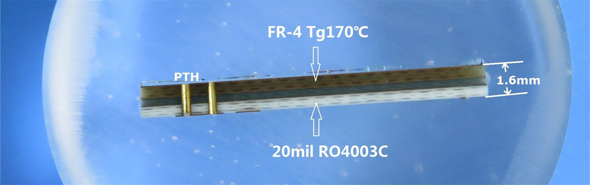
3) Dielectric Thickness: We provide designers with extensive flexibility through a wide array of dielectric thicknesses, including 0.5mm, 0.8mm, 1.0mm, 1.2mm, 1.5mm, 2.0mm, 3.0mm, 4.0mm, 5.0mm, 6.0mm, 7.0mm, 8.0mm, 10.0mm, and 12.0mm.
4) Panel Size: Due to the constraints of the base laminate size, the maximum finished PCB dimensions we can provide are 150mm x 220mm.
5) Solder Mask: Aesthetic and functional customization is available through a selection of solder mask colors, such as green, black, blue, yellow, and red.
6) Surface Finish: We support a comprehensive range of surface finishes to meet diverse assembly and performance requirements, including Bare Copper, HASL (Hot Air Solder Leveling), ENIG (Electroless Nickel Immersion Gold), Immersion Silver, Immersion Tin, OSP (Organic Solderability Preservative), Pure Gold, and ENEPIG (Electroless Nickel Electroless Palladium Immersion Gold).

Diverse Application Spectrum
The robust combination of electrical and mechanical properties makes TP High Frequency PCBs indispensable in several high-stakes industries. A typical example is a 1.5mm thick TP PCB with an OSP (Organic Solderability Preservative) surface finish, commonly used in sophisticated communication systems. Beyond this, these PCBs are critically deployed in applications such as the Beidou satellite navigation system, missile-borne guidance systems, advanced radar fuzes, and miniaturized high-gain antennas. In each case, the material's stable electrical performance, thermal resilience, and reliability under harsh conditions ensure optimal system functionality.
Conclusion
For engineers pushing the boundaries of high-frequency and high-speed design, custom TP PCB offers a powerful combination of customizability, performance, and reliability. By enabling precise control over dielectric properties and providing robust performance in challenging environments, it serves as a foundational component for the next generation of aerospace, defense, and telecommunications technology. When your design demands uncompromising signal integrity, TP material provides a proven and capable solution.
Categories
New Blog
Tags
 6-11C Shidai Jingyuan, Fuyong, Baoan, Shenzhen, Guangdong, China 518103


For inquiries about our products or pricelist, please leave to us and we will be in touch within 24 hours.
© Copyright: 2026 Shenzhen Bicheng Electronics Technology Co., Ltd.. All Rights Reserved.

IPv6 network supported


