
 Call Us Now !
Tel : +86 755 27374946
Call Us Now !
Tel : +86 755 27374946
 Order Online Now !
Email : info@bichengpcb.com
Order Online Now !
Email : info@bichengpcb.com
What is the Dk and Df of the F4BTMS615 Material at 10 GHz?
What is the Dk and Df of the F4BTMS615 Material at 10 GHz?
In the world of RF (Radio Frequency) and microwave engineering, the substrate material upon which a circuit is printed is not merely a passive carrier; it is an active participant in the circuit's performance. When designing for frequencies in the GHz range, two material parameters rise above all others in importance: the Dielectric Constant (Dk) and the Dissipation Factor (Df).
For engineers and technical procurement specialists evaluating materials for aerospace, radar, or satellite communication systems, the question is rarely just "What is the Dk?" but rather, "How stable is this Dk, and how low is the loss at my operating frequency?"
This article provides an in-depth analysis of the F4BTMS615 PCB, focusing specifically on its electrical properties at 10 GHz, and explains how its material construction and physical design translate into high-frequency performance.
The Core Answer: Dk and Df at 10 GHz
To address the primary technical question directly: For the F4BTMS615 material, at a test frequency of 10 GHz, the critical parameters are as follows:
While these numbers provide a snapshot, understanding why these values matter, and how they are achieved, requires a deeper look into the material science and the physical construction of the PCB.

Deconstructing Dielectric Constant (Dk) at 6.15
A Dk of 6.15 at 10 GHz tells us that this is a high-Dk material compared to standard substrates like FR4 (typically ~4.5) or even some conventional PTFE laminates.
Why Choose a Dk of 6.15?
From a design perspective, a higher Dk means that the wavelength of the RF signal is shortened as it travels through the medium. This allows for circuit miniaturization. Transmission lines, matching networks, and antenna elements can be physically smaller while maintaining the same electrical length. For aerospace and military radar applications where space is at a premium, this is a distinct advantage.
The Stability Behind the Number
However, a Dk value is only useful if it remains stable. The F4BTMS615 achieves this stability through its unique material formulation. As outlined in the product introduction, this material is a composite of PTFE resin, a significant amount of uniformly distributed nano-ceramics, and ultra-thin glass fiber cloth.
The nano-ceramics are the primary drivers of the high Dk, but their uniform distribution is key to minimizing Dk variation across the board. Furthermore, the material specification highlights a Thermal Coefficient of Dk of -96 ppm/°C. This means that across a massive temperature range (-55°C to 150°C), the Dk remains virtually unchanged. For a phased array antenna operating in the fluctuating thermal environment of an aircraft or satellite, this stability prevents "beam squint" or frequency drift, ensuring the system performs as designed regardless of the conditions.
The Significance of a 0.0020 Dissipation Factor (Df)
The Dissipation Factor, or Df, is a measure of signal loss within the dielectric material. The lower the number, the less energy is converted to heat and lost. At 10 GHz, a Df of 0.0020 is considered excellent and places the F4BTMS615 firmly in the category of "low-loss" materials.
Implications for System Design
Why does a Df of 0.0020 matter in practice?
The Role of Material Purity
The low Df is a direct result of the base resin and the reinforcement strategy. Traditional glass fiber can be a source of loss at high frequencies. The F4BTMS PCB series mitigates this by using ultra-thin, ultra-fine glass fiber cloth and a "significant amount" of ceramics. This combination minimizes the "negative effects of glass fiber on electromagnetic wave propagation," as stated in the product notes. Additionally, the use of RTF (Reverse Treated Foil) low roughness copper foil is critical. Rough copper surfaces can trap signal energy, effectively increasing conductor loss. The RTF foil provides excellent adhesion while presenting a smoother surface to the signal, ensuring that the total loss (dielectric + conductor) is kept to a minimum.
How the PCB Construction Supports High-Frequency Performance
The raw laminate properties are only half the story. The way the PCB is fabricated must preserve these characteristics. The construction details of this specific F4BTMS615 PCB are designed with RF performance in mind.
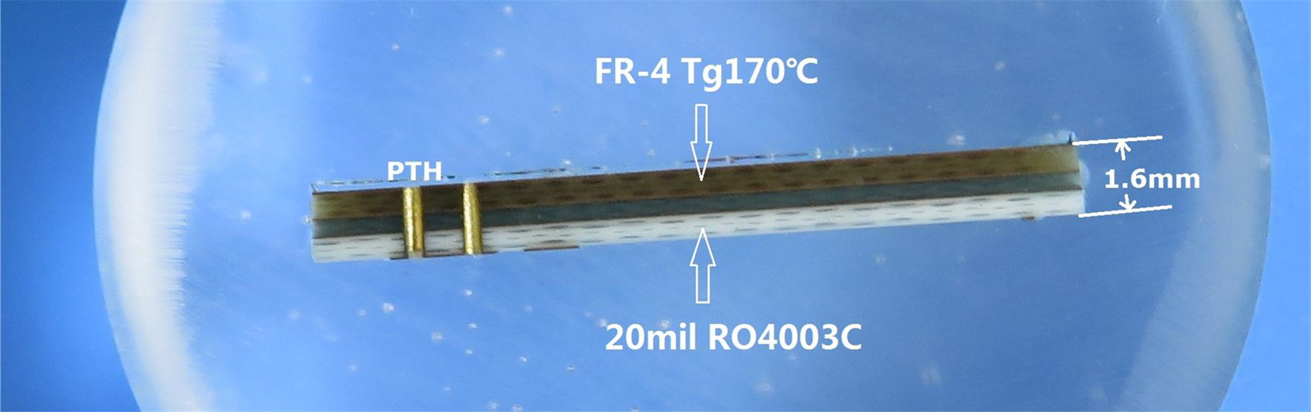
The 2-Layer Stackup
The Deliberate Absence of Solder Mask
One of the most telling details in the construction is the specification: "Top Solder Mask: No" and "Bottom Solder Mask: No."
Why? Standard solder mask materials are lossy and poorly characterized at GHz frequencies. Applying solder mask over an RF trace can change its impedance and introduce significant loss. By omitting it, the PCB exposes the bare copper (protected by the Immersion Tin finish), ensuring that the signal propagates strictly through the air and the stable F4BTMS615 dielectric, just as the simulation software intended. This "bare" approach is a hallmark of high-quality microwave PCBs.
Immersion Tin Finish
The choice of Immersion Tin over more common finishes like ENIG is also noteworthy for RF design. It provides a perfectly flat surface for component placement, which is essential for the 27 SMT pads on the board. A flat finish minimizes signal reflections at component interconnects, preserving the integrity of the high-frequency waveforms.
From Data to Application: Where This Matters
The combination of a stable Dk of 6.15 and a low Df of 0.0020 makes this PCB suitable for the most demanding applications listed in your specifications:
Quality and Assurance
To ensure that the theoretical Dk and Df values translate into real-world performance, every board undergoes 100% Electrical Testing. This verifies impedance control and continuity, ensuring that the complex RF nets (of which there are 2 main nets, but 35 vias for grounding) function correctly. Manufactured to IPC-Class-2 standards, this board offers the reliability required for dedicated service electronic products.
Conclusion
The Wangling F4BTMS615 PCB is more than just a set of specifications. Its Dk of 6.15 and Df of 0.0020 at 10 GHz are the result of a sophisticated material design that combines nano-ceramic fillers with advanced PTFE resins and low-profile copper. When paired with a fabrication process that omits lossy solder mask and utilizes immersion tin, the result is a high-reliability, high-performance platform suitable for the world's most challenging RF environments, from military radar to satellite communications.
Categories
New Blog
Tags
 6-11C Shidai Jingyuan, Fuyong, Baoan, Shenzhen, Guangdong, China 518103


For inquiries about our products or pricelist, please leave to us and we will be in touch within 24 hours.
© Copyright: 2026 Shenzhen Bicheng Electronics Technology Co., Ltd.. All Rights Reserved.

IPv6 network supported


