
 Call Us Now !
Tel : +86 755 27374946
Call Us Now !
Tel : +86 755 27374946
 Order Online Now !
Email : info@bichengpcb.com
Order Online Now !
Email : info@bichengpcb.com
What Is Your Minimum Drill Hole Size?
What Is Your Minimum Drill Hole Size?
A Comprehensive Guide to PCB Drilling Capabilities
When designing a printed circuit board (PCB), one critical specification engineers must consider is the minimum drill hole size. This parameter determines the feasibility of vias, through-holes, and microvias, directly impacting the board’s functionality, density, and cost.
In this article, we’ll explore:
- Standard vs. laser drill hole sizes (0.2mm mechanical vs. 0.1mm laser for HDI)
- How material selection affects drilling precision (e.g., F4BM220 laminates)
- Key considerations for high-frequency and RF applications
- Real-world PCB examples with drilling constraints
Understanding Minimum Drill Hole Sizes: Mechanical vs. Laser Drilling
1. Standard Mechanical Drilling (≥0.2mm)
Mechanical drilling is the most common method for creating through-holes in PCBs. The standard minimum drill size is 0.2mm (8 mils), though some manufacturers can achieve 0.15mm (6 mils) with high-precision equipment.
Limitations:
- Aspect ratio constraints (drill depth vs. diameter)
- Potential for drill breakage with ultra-small holes
- Material-dependent performance (e.g., fiberglass-reinforced laminates vs. PTFE-based materials)
Example PCB with Mechanical Drilling:
- Minimum Hole Size: 0.3mm (12 mils)
- Layer Count: 2
- Base Material: F4BM220 (PTFE-based, low-loss)
- Finished Thickness: 1.7mm
- Plating Thickness: 20µm
This design suits RF/microwave applications where larger vias are acceptable, and signal integrity is prioritized over ultra-high density.
2. Laser Drilling for HDI PCBs (≥0.1mm)
High-Density Interconnect (HDI) PCBs require laser drilling to achieve microvias as small as 0.1mm (4 mils). This method is essential for:
- Smartphones, wearables, and compact electronics
- High-speed digital circuits (e.g., 5G modules)
- RF systems needing buried/blind vias
Advantages of Laser Drilling:
- No physical drill wear (longer tool life)
- Tighter tolerances (±0.025mm)
- Suitable for flexible andrigid-flex PCBs
However, laser drilling is more expensive and may require specialized materials (e.g., low-Dk laminates like F4BM220 for minimal signal loss).
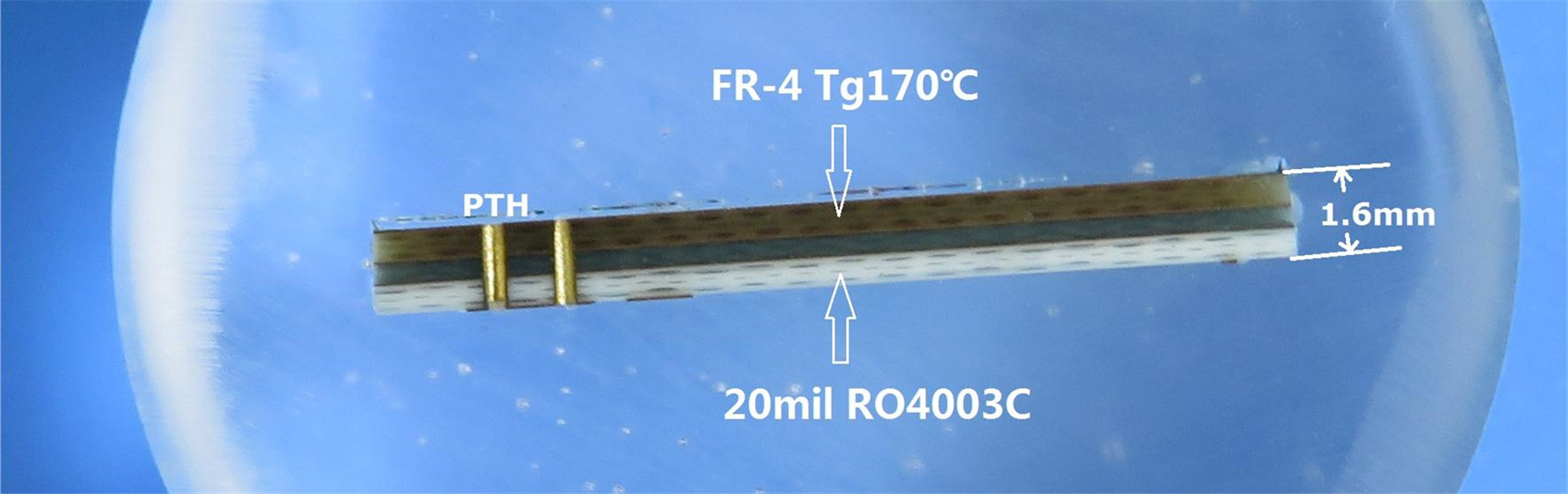
How PCB Material Affects Drill Hole Size & Performance
The choice of substrate plays a crucial role in determining achievable hole sizes and signal performance.
Case Study: F4BM220 PTFE Laminate
Our F4BM220 material is engineered for high-frequency applications with:
- Dielectric Constant (Dk): 2.2±0.04 @ 10GHz
- Dissipation Factor (Df): 0.001 @ 10GHz
- Low Moisture Absorption (≤0.08%)

Why This Matters for Drilling:
✔Thermal Stability (CTE: 25 ppm/°C in X/Y-axis) reduces hole wall deformation during drilling.
✔Low Dk/Df ensures minimal signal loss in high-speed/RF designs.
✔Compatibility with both mechanical and laser drilling (unlike some ceramics).
Comparison with FR-4:
|
Parameter |
F4BM220 (PTFE) |
Standard FR-4 |
|
Min Hole Size |
0.1mm (laser) |
0.2mm (mech.) |
|
Dk @ 10GHz |
2.2 |
4.3-4.8 |
|
Df @ 10GHz |
0.001 |
0.02 |
|
Thermal Stability |
Excellent |
Moderate |
For microwave antennas, satellite comms, and radar systems, F4BM220 PCB ensures better signal integrity than FR-4, even with smaller vias.
Design Considerations for Optimal Drill Hole Sizes
1. Aspect Ratio & Reliability
- Standard PCBs: Max aspect ratio of 10:1 (e.g., 1.7mm board thickness→min hole size ~0.17mm).
- HDI PCBs: Can exceed 1:1 ratio with stacked microvias.
2. Plating Quality (Critical for High-Frequency PCBs)
- Via plating thickness≥20µm (ensures conductivity in RF circuits).
- ENIG surface finish (prevents oxidation in harsh environments).
3. Cost vs. Performance Trade-offs
- Laser drilling adds ~20-30% cost but enables smaller form factors.
- Mechanical drilling is economical for larger boards (e.g., our 130.5mm x 103mm example).
Conclusion: Choosing the Right Drill Size for Your PCB
The minimum drill hole size depends on:
✅Manufacturing method (mechanical: 0.2mm; laser: 0.1mm)
✅Material properties (PTFE vs. FR-4)
✅Application needs (RF vs. digital)
For high-frequency designs, our F4BM220 PCBs offer:
- Low-loss signal transmission
- Stable mechanical drilling down to 0.3mm
- Superior thermal performance
Need a custom solution? Contact us for expert guidance on optimizing your PCB’s drill sizes and stackup!
Categories
New Blog
Tags
 6-11C Shidai Jingyuan, Fuyong, Baoan, Shenzhen, Guangdong, China 518103


For inquiries about our products or pricelist, please leave to us and we will be in touch within 24 hours.
© Copyright: 2026 Shenzhen Bicheng Electronics Technology Co., Ltd.. All Rights Reserved.

IPv6 network supported


