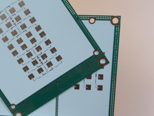
How Do You Handle PCB Panelization?
PCB Panelization: Optimizing Panel Size for Cost-Efficiency (V-Cut vs. Tab Routing)
Introduction
In PCB manufacturing, panelizationis a critical step that directly impacts production efficiency, material utilization, and overall cost. Panelization involves arranging multiple PCB designs onto a single manufacturing panel to optimize fabrication and assembly processes. The two most common methods for separating individual PCBs from the panel areV-cut scoringandtab routing with breakaway tabs.
This article explores best practices for PCB panelization, focusing on how we optimize panel sizes for cost-efficiency while maintaining structural integrity and electrical performance. We’ll also highlight how our high-frequency Rogers RO3003 PCB benefit from precise panelization techniques.
Why PCB Panelization Matters
Panelization maximizes material usage, reduces handling time, and improves assembly efficiency. Without proper panelization, manufacturers risk:
-Higher material waste–Poor panel design leads to unused board space.
-Increased assembly costs–Manual handling of small PCBs slows down production.
-Lower structural stability–Thin or high-frequency PCBs (like Rogers RO3003) require careful panelization to avoid warping or cracking.
By optimizing panel size and separation methods, we ensure cost-effective, high-yield production—especially for advanced applications like automotive radar, 5G infrastructure, and RF communications.
V-Cut vs. Tab Routing: Choosing the Right Method
1. V-Cut (Scoring) Panelization
Best for:Straight-line separations,rigid PCBs, and high-volume production.
How it works:
- A V-shaped groove is cut partially through the PCB panel, leaving a thin connecting layer.
- After assembly, boards are snapped apart along the V-cut lines.
Advantages:
-Fast separation–Ideal for automated assembly lines.
-Clean edges–Minimal post-processing required.
-Space-efficient–Allows tighter PCB placement.
Limitations:
-Not suitable for complex shapes–Only works for straight-line separations.
-Risk of stress fractures–Thin or flexible PCBs (like our 0.2mm RO3003 boards) may require additional support.
2. Tab Routing (Breakaway Tabs)
Best for:Irregular PCB shapes, flexible circuits, and high-frequency boards.
How it works:
- Small perforated tabs (mouse bites) hold PCBs in place within the panel.
- After assembly, boards are broken free by applying pressure.
Advantages:
-Flexible design–Supports complex PCB outlines.
-Better for thin PCBs–Reduces stress on delicate materials like Rogers RO3003.
-No sharp edges–Minimizes risk of damage during handling.
Limitations:
-Requires manual de-panelization–Slower than V-cut for high-volume orders.
-May need additional finishing–Breakaway tabs can leave small protrusions.
Optimizing Panel Size for Cost Efficiency
To maximize cost savings, we consider:
1. Material Utilization
-Standard panel sizes(e.g., 18"x24", 21"x24") minimize waste.
- Our 69.25mm x 92.45mm RO3003 PCBs are strategically arranged to maximize yield.
2. Assembly Compatibility
- Panels must fit pick-and-place machines and reflow ovens.
-High-frequency PCBs (like RO3003 PCB) require careful handling to avoid impedance variations.
3. Breakaway Method Selection
-V-cut for simple, rigid boards→Faster production.
-Tab routing for complex, thin boards→Prevents cracking.
Case Study: High-Frequency Rogers RO3003 PCB Panelization
Our 2-laye rRogers RO3003 PCB is designed for RF and microwave applications, where precision and material stability are critical.
Key Specifications:
-Base Material:Rogers RO3003 (ceramic-filled PTFE)
-Dimensions:69.25mm x 92.45mm (2 types, 2 pieces per panel)
-Thickness:0.2mm (ultra-thin for high-frequency performance)
-Surface Finish:Immersion Gold (optimal for RF signal integrity)
-Trace/Space:5/5 mils (high-density routing)

Why Panelization Matters for RO3003 PCBs:
-Thermal Stability: Rogers 3003 has a low CTE (17 ppm/°C in X/Y axis), reducing warping risk during depaneling.
-High-Frequency Performance:Proper panelization ensures consistent dielectric properties (Dk = 3.0±0.04).
-Cost Efficiency:Optimized panel layouts reduce material waste, lowering production costs.
Best Practices for PCB Panelization
1.Minimize Waste–Use CAD software to optimize PCB arrangement.
2.Consider Depaneling Method Early–Choose V-cut or tab routing during design.
3.Account for Tooling Holes–Ensure panels fit assembly equipment.
4.Test Electrical Continuity–Our100% electrical testing ensures reliability post-panelization.
Conclusion
Effective PCB panelization balances cost-efficiency, manufacturability, and performance. For high-frequency PCBs like Rogers RO3003 PCB, selecting the right depaneling method (V-cut or tab routing) ensures structural integrity and electrical stability.
As a trusted PCB supplier, we optimize panelization for maximum yield and minimal waste, delivering high-performance boards for 5G, automotive radar, and RF applications.
Need a cost-optimized PCB solution? Contact us today for a panelization strategy tailored to your design!

 Call Us Now !
Tel : +86 755 27374946
 Order Online Now !
Email : info@bichengpcb.com


