
 Call Us Now !
Tel : +86 755 27374946
Call Us Now !
Tel : +86 755 27374946
 Order Online Now !
Email : info@bichengpcb.com
Order Online Now !
Email : info@bichengpcb.com
Why Does an 8mil ENEPIG High-Frequency PCB Matter for RF Design?
Meta Description: An engineering deep-dive into WL-CT615 hydrocarbon-ceramic PCB with 8mil dielectric core and ENEPIG finish — material data, design trade-offs, and application guidance for RF and hardware engineers.
RF engineers face a persistent tension: shrinking form factors versus signal integrity. When a board must fit into an antenna feed or radar frontend while carrying signals at 10 GHz and beyond, every dielectric choice and surface finish becomes a decision with measurable consequences. This article examines the engineering rationale behind ultra-thin high-frequency PCBs built on WL-CT615 hydrocarbon-ceramic laminate with an 8mil (0.203 mm) core and ENEPIG finish — and what the material data means for real RF design.
At the heart of any high-frequency PCB is the dielectric. WL-CT615 is a thermosetting hydrocarbon-resin laminate reinforced with fiberglass cloth and loaded with ceramic fillers. This three-part system is deliberate: the hydrocarbon resin provides a low-polarity matrix (dissipation factor of 0.004 at 10 GHz), ceramic fillers raise the dielectric constant to 6.15 (typical at 10 GHz), and fiberglass ensures dimensional stability through lamination and reflow.
What distinguishes this material from PTFE alternatives is processability. PTFE laminates require specialized etching, bonding, and drilling, with poorer dimensional stability under thermal cycling. Wangling WL-CT615's thermosetting system fabricates on conventional FR-4 lines, yielding higher consistency and lower cost without sacrificing RF performance. Thermal-mechanical data supports this: Tg exceeds 280°C, decomposition is 398°C, X/Y CTE of 15/17 ppm/°C matches copper (~17 ppm/°C), and Z-axis CTE of 33 ppm/°C keeps plated through-holes reliable under cycling. Thermal conductivity of 0.72 W/m·K aids heat dissipation in power amplifiers. The material is halogen-free, UL-94 V-0 rated, and supports long-term use from -55°C to +260°C.
The 8mil (0.203 mm) core is the thinnest standard WL-CT615 offering, imposing both opportunities and constraints.
On the opportunity side, an 8mil core with 1oz (35 µm) copper on both sides yields a finished board of approximately 0.3 mm — fitting compact antenna modules, LNB downconverters, and sensor frontends where height is a hard constraint. The high Dk of 6.15 further enables miniaturization: resonator and antenna element sizes scale inversely with the square root of Dk, reducing circuit footprint.
On the constraint side, a thin dielectric raises characteristic impedance for a given trace width. Designers targeting 50 Ω need narrower traces, which the 4/5 mil minimum trace/space capability supports — but at the cost of increased conductor loss and reduced current margin. The Dk tolerance of ±0.15 and TCDK of -122 ppm/°C must be factored into impedance simulations, especially for filters across wide temperature ranges. The 8mil thickness tolerance of ±0.025 mm (±1.0 mil) is the tightest in the line, benefiting impedance-critical designs, though corner-case simulations at tolerance extremes remain advisable.
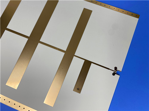
Surface finish is often treated as a manufacturing afterthought, but for high-frequency assemblies it directly affects solder joint integrity, signal loss, and yield.
ENEPIG (Electroless Nickel Electroless Palladium Immersion Gold) deposits three layers: nickel for corrosion resistance and hardness, palladium as a barrier against "black pad" defects, and immersion gold for solderability. The palladium layer is the key differentiator from ENIG, which lacks this barrier and is susceptible to black pad — a brittle, non-wetting interface causing intermittent failures.
For RF assemblies, ENEPIG offers three practical advantages:
· Multiple reflow compatibility: withstands repeated thermal cycles without losing solderability, critical for multi-pass SMT.
· Flat coplanar surface: unlike HASL's uneven coating, ENEPIG provides a uniformly flat surface ideal for fine-pitch RF ICs.
· Wire-bonding capability: supports reliable gold and aluminum wire bonding for RF IC attachments in microwave modules.
The trade-off is cost — ENEPIG exceeds HASL and typically ENIG. Where multiple reflow, fine-pitch assembly, or wire bonding is required, the premium is justified; for simple single-reflow consumer boards, HASL or ENIG may suffice.
A 2-layer ENEPIG PCB is not universal. Designers should weigh several factors.
· Layer Count and Routing
A 2-layer board limits routing complexity and ground plane integrity. For circuits requiring tight RF-digital isolation or multiple impedance-controlled lines, a 4-layer+ stackup may be necessary. The reference design has 31 components across 69 pads and 2 nets — intentionally simple, suited to an antenna feed or single-function RF module, not a complex transceiver.
· Via Strategy
This board uses through-hole vias only (20 µm plating, 0.4 mm minimum hole). Through-hole stubs cause reflections at microwave frequencies. Above ~3 GHz, stub length should be controlled or back-drilled — unavailable in this 2-layer config. Account for via parasitics in electromagnetic simulations.
· Thermal Management
While 0.72 W/m·K conductivity is respectable, a 0.3 mm board has limited thermal mass. For power amplifiers dissipating significant heat, consider thermal vias, copper pours, or the aluminum-backed WL-CT615-AL variant (180 W/m·K).
· Quality Standards
Built to IPC-6012 Class 2 with 100% electrical testing before shipment. Class 2 suits commercial and industrial products; for aerospace or medical requiring Class 3, specify upgraded criteria at ordering.
Based on the material and construction data, this PCB class is well-suited for:
· Base station and satellite antenna feeds requiring compact size and controlled impedance.
· 24 GHz and 77 GHz automotive radar frontends needing low-loss, temperature-stable dielectrics.
· LNB and downconverter circuits where Df of 0.004 at 10 GHz minimizes attenuation.
· RF filters and resonators benefiting from 6.15 Dk for size reduction and -122 ppm/°C stability.
· Power amplifier modules where 0.72 W/m·K thermal conductivity aids heat dissipation.
It is less appropriate for complex multi-function transceivers, high-layer-count mixed-signal designs, or applications requiring Class 3 without customization. Note that RTF copper (superior PIM performance, lower conductor loss) is available for other WL-CT grades but not WL-CT615, which ships exclusively with ED copper foil in 0.5 oz and 1 oz.
Q: What is the minimum trace width on an 8mil WL-CT615 PCB?
A: The minimum trace/space is 4/5 mils (0.10/0.13 mm). For a 50 Ω microstrip on an 8mil core with Dk 6.15, the required trace width is narrower than on thicker or lower-Dk substrates, so verify your target impedance falls within the 4 mil minimum.
Q: How does ENEPIG affect insertion loss at microwave frequencies?
A: ENEPIG's flat, uniform surface minimizes roughness-related conductor loss versus HASL. The gold layer is thin (0.03–0.08 µm), so skin-depth effects at 10 GHz are dominated by underlying nickel and palladium. For critical paths, request insertion loss test coupons on the actual panel.
Q: Can WL-CT615 be used for aerospace applications?
A: WL-CT615 exhibits radiation resistance and low outgassing, meeting aerospace vacuum requirements. However, the standard PCB is IPC-6012 Class 2. For flight hardware, specify Class 3, thermal cycling qualification, and material lot traceability at ordering.
The WL-CT615 PCB 8mil ENEPIG Finish is a targeted engineering solution, not a general-purpose board. Its 6.15 Dk hydrocarbon-ceramic core, 0.3 mm ultra-thin profile, and ENEPIG finish address specific RF challenges — miniaturization, signal integrity, and assembly reliability — with measurable data backing each claim. Designers who understand the trade-offs between thin dielectrics and trace width, ENEPIG cost and reflow compatibility, and 2-layer simplicity and routing flexibility can determine fit. For those seeking a cost-effective, FR-4-processable alternative to PTFE boards in compact RF modules, the data supports serious consideration.
Categories
New Blog
Tags
 6-11C Shidai Jingyuan, Fuyong, Baoan, Shenzhen, Guangdong, China 518103


For inquiries about our products or pricelist, please leave to us and we will be in touch within 24 hours.
© Copyright: 2026 Shenzhen Bicheng Electronics Technology Co., Ltd.. All Rights Reserved.

IPv6 network supported


