

 Call Us Now !
Tel : +86 755 27374946
Call Us Now !
Tel : +86 755 27374946
 Order Online Now !
Email : info@bichengpcb.com
Order Online Now !
Email : info@bichengpcb.com
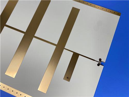
The WL-CT615 PCB 8mil ENEPIG Finish represents a carefully engineered solution for high-frequency, space-constrained electronic designs.
Item NO.:
BIC-619-v704Order(MOQ):
1-10Payment:
T/TProduct Origin:
ChinaShipping Port:
ShenzhenLead Time:
7-10 days
Wangling WL-CT615 8mil Ultra-Thin High-Frequency 2-Layer PCB ENEPIG Finish
This article provides a comprehensive technical profile of the WL-CT615 PCB, anultra-thin 2-layer high-frequency circuit board built on Wangling WL-CT615 hydrocarbon-ceramic laminate with an 8mil (0.203 mm) dielectric core and ENEPIG surface finish.
Part I details the PCB construction, layer stackup, electrical statistics, ENEPIG finish technology, quality assurance standards, and target applications.
Part II presents an in-depth technical profile of the WL-CT615 copper-clad laminate itself, including a complete datasheet, dielectric thickness options, material composition, availability specifications, and a product image. The two sections are kept independent to avoid repetition.
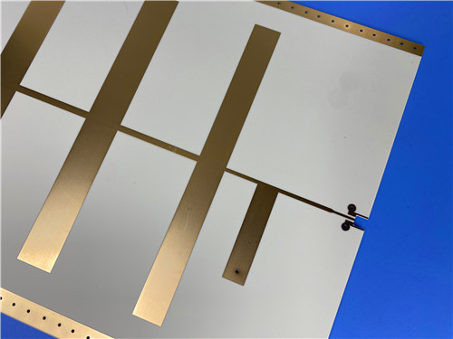
The WL-CT615 PCB is a 2-layer rigid high-frequency printed circuit board engineered for applications demanding controlled impedance, low signal loss, and a compact form factor. It is built on Wangling's WL-CT615 organic polymer ceramic fiberglass-clad laminate — a thermosetting hydrocarbon-resin-based high-frequency material — which combines a dielectric constant (Dk) of 6.15 at 10 GHz with a dissipation factor (Df) of just 0.004. These properties make the board well-suited for RF and microwave circuit designs where miniaturization and signal integrity are critical.
With a finished board thickness of only 0.3 mm and a core dielectric of 8mil (0.203 mm), this Wangling PCB achieves an exceptionally low profile while maintaining structural rigidity. The outer layers feature 1oz (35 μm) finished copper weight, providing adequate current-carrying capacity for most RF and low-power digital circuits. Each board measures 99.03 mm × 45.6 mm with a dimensional tolerance of ±0.15 mm, and is manufactured to IPC-6012 Class 2 acceptance standards with 100% electrical testing prior to shipment.
The table below summarizes the core construction parameters of the WL-CT615 8mil PCB, covering dimensions, material finishes, drilling capability, and manufacturing tolerances.
|
Parameter |
Specification |
|
Board Dimensions |
99.03 mm × 45.6 mm (1 PCS), ±0.15 mm |
|
Finished Board Thickness |
0.3 mm |
|
Minimum Trace / Space |
4 / 5 mils |
|
Minimum Hole Size |
0.4 mm |
|
Via Type |
Through-hole only (no blind vias) |
|
Via Plating Thickness |
20 μm |
|
Finished Cu Weight (Outer Layers) |
1 oz (35 μm / 1.4 mils) |
|
Surface Finish |
ENEPIG |
|
Top / Bottom Solder Mask |
Green / Green |
|
Top / Bottom Silkscreen |
White / White |
|
Electrical Test |
100% tested prior to shipment |
|
Accepted Standard |
IPC-6012 Class 2 |
|
Artwork Format |
Gerber RS-274-X |
|
Availability |
Worldwide |
The stackup consists of a symmetric 2-layer rigid structure with 35 μm copper on both outer layers and an 8mil (0.203 mm) WL-CT615 dielectric core, as detailed below.
|
Layer |
Thickness / Material |
|
Layer 1 — Copper (Top) |
35 μm (1 oz) |
|
Core Dielectric — WL-CT615 |
0.203 mm (8 mils) |
|
Layer 2 — Copper (Bottom) |
35 μm (1 oz) |
The board contains 31 components across 69 total pads, with 56 vias connecting 2 electrical nets — reflecting a moderately dense yet straightforward 2-layer design.
|
Metric |
Count |
|
Components |
31 |
|
Total Pads |
69 |
|
Through-Hole Pads |
41 |
|
Top SMT Pads |
28 |
|
Bottom SMT Pads |
0 |
|
Vias |
56 |
|
Nets |
2 |
The Electroless Nickel Electroless Palladium Immersion Gold (ENEPIG) surface finish is a premium metallization choice that offers several advantages over conventional ENIG (Electroless Nickel Immersion Gold) or HASL finishes. ENEPIG deposits a layer of electroless nickel, followed by a thin layer of electroless palladium, and finally immersion gold. The palladium layer acts as a barrier that prevents nickel corrosion and "black pad" defects — a known reliability concern associated with ENIG finishes.
For high-frequency PCBs, ENEPIG provides excellent solderability for multiple reflow cycles, flat coplanar surfaces ideal for fine-pitch SMT components, and reliable wire-bonding capability for RF IC attachments. The nickel layer offers good corrosion resistance and a hard, durable surface, while the thin gold layer ensures long-term solderability and oxidation resistance. This finish is particularly well-suited for high-reliability RF and microwave assemblies where consistent signal paths and multiple assembly passes are required.
Every WL-CT615 high frequency PCB undergoes 100% electrical testing (flying probe or fixture-based) prior to shipment, ensuring all nets are continuous and free of opens or shorts. The boards are manufactured to IPC-6012 Class 2 specifications, which define performance requirements for rigid printed boards including copper plating thickness, solder mask adhesion, dimensional stability, and dielectric integrity. Class 2 is appropriate for most commercial and industrial electronic products where consistent performance and extended service life are expected.
The use of Gerber RS-274-X artwork format ensures fabrication data compatibility with global PCB manufacturing infrastructure, and the product is available for worldwide shipping.
The WL-CT615 2-layer PCB's combination of high Dk, low loss, ultra-thin profile, and ENEPIG finish makes it suitable for a range of high-frequency applications:
• Base station antennas and satellite antennas: High-Dk materials enable compact antenna element designs with controlled radiation patterns.
• Automotive radar, sensors, and navigation systems: Low-loss dielectric and temperature-stable Dk support reliable 24 GHz and 77 GHz radar frontends.
• Power amplifiers: The 0.72 W/m·K thermal conductivity of the core material aids heat dissipation in power amplifier circuits.
• Satellite high-frequency heads (LNBs): Low Df minimizes signal attenuation in downconverter circuits.
• RF devices and filters: High Dk reduces resonator size, while a TCDK of -122 ppm/°C ensures filter performance across temperature extremes.
• WiMAX antennas and distributed antenna systems: Controlled impedance and low loss support reliable broadband signal distribution.
The WL-CT615 PCB 8mil ENEPIG Finish represents a carefully engineered solution for high-frequency, space-constrained electronic designs. Its 0.3 mm ultra-thin rigid construction, 6.15 Dk hydrocarbon-ceramic core, 4/5 mil fine-line capability, and premium ENEPIG surface finish collectively deliver a board that balances miniaturization, signal integrity, and assembly reliability. Manufactured to IPC-6012 Class 2 standards with 100% electrical testing and available worldwide, this PCB is a practical choice for RF modules, antenna feeds, filters, and sensor frontends. For designers seeking a cost-effective alternative to PTFE-based high-frequency boards, the WL-CT615 PCB offers FR-4-like processability combined with genuinely high-frequency material properties.
Part II: WL-CT615 Copper-Clad Laminate (CCL)
In-Depth Material Technical Profile
The WL-CT615 is a high-frequency copper-clad laminate manufactured by Taizhou Wangling Insulating Materials Factory . It belongs to the WL-CT series of organic polymer ceramic fiberglass-clad laminates, which are thermosetting resin-based high-frequency materials. The dielectric layer composition consists of hydrocarbon resin, ceramic fillers, and fiberglass cloth reinforcement — a formulation that delivers low-loss performance suitable for high-frequency designs while maintaining PCB processability comparable to standard FR-4 materials.
Unlike PTFE (Teflon)-based high-frequency laminates, which require specialized processing conditions and exhibit poorer dimensional stability, the WL-CT615's thermosetting hydrocarbon-ceramic system can be processed using conventional FR-4 fabrication techniques. This significantly simplifies PCB manufacturing, improves circuit consistency and yield, and reduces overall production cost — making it a viable substitute for comparable imported high-frequency laminate products. The WL-CT series offers dielectric constants ranging from 3.00 to 6.15, with WL-CT615 representing the highest-Dk grade in the series at 6.15 (typical at 10 GHz).
The WL-CT615's dielectric system combines three key components:
• Hydrocarbon resin: A thermosetting polymer matrix that provides low dielectric loss, excellent moisture resistance, and high thermal stability. The hydrocarbon chemistry is inherently low-polarity, which translates directly to a low dissipation factor at microwave frequencies.
• Ceramic fillers: High-Dk ceramic particles dispersed throughout the resin matrix raise the overall dielectric constant to 6.15 (typical at 10 GHz) while contributing to improved thermal conductivity (0.72 W/m·K) and a reduced coefficient of thermal expansion.
• Fiberglass cloth: Provides mechanical reinforcement and dimensional stability, ensuring the laminate maintains flatness and structural integrity through multiple lamination cycles and thermal excursions.
The combination of hydrocarbon resin and composite ceramics yields excellent low-loss characteristics, high-temperature resistance, and temperature stability. The material exhibits a stable temperature coefficient of dielectric constant (TCDK) of -122 ppm/°C, a low thermal expansion coefficient, and a glass transition temperature (Tg) exceeding 280°C. It is also halogen-free and achieves a UL-94 V-0 flame retardancy rating.
• Low Dk tolerance and low loss: Dk tolerance of ±0.15 ensures consistent impedance control across production lots; Df of 0.004 at 10 GHz minimizes signal attenuation.
• Hydrocarbon-ceramic thermosetting resin system: Delivers superior PCB processability and thermal resistance compared to thermoplastic high-frequency materials.
• Excellent Dk temperature stability: TCDK of -122 ppm/°C means minimal impedance drift across operating temperature ranges.
• CTE matched to copper: X-axis CTE of 15 ppm/°C and Y-axis of 17 ppm/°C closely match copper's CTE (~17 ppm/°C), while Z-axis CTE of 33 ppm/°C ensures reliable plated through-hole integrity under thermal cycling.
• High Tg (>280°C): Maintains dimensional stability and hole-copper quality at elevated temperatures, supporting lead-free reflow profiles.
• High thermal conductivity (0.72 W/m·K): Outperforms comparable thermoplastic materials, making it suitable for high-power applications.
• Commercial, high-volume, cost-effective: Produced at scale with competitive pricing relative to imported alternatives.
• Excellent radiation resistance: Maintains stable dielectric and physical properties after radiation exposure, suitable for aerospace and space applications.
• Low outgassing: Meets aerospace vacuum outgassing requirements when tested per standard vacuum volatilization methods.
The following table presents the complete technical datasheet for the WL-CT615 laminate, covering electrical, thermal, mechanical, and chemical properties with specified test conditions and units. All values are typical measurements intended to assist material selection.
|
Property |
Test Condition |
Unit |
WL-CT615 Value |
|
Dielectric Constant (Typical) |
10 GHz |
— |
6.15 |
|
Dielectric Constant (Design) |
10 GHz |
— |
6.4 |
|
Dk Tolerance |
— |
— |
±0.15 |
|
Dissipation Factor (Typical) |
2 GHz |
— |
0.0032 |
|
Dissipation Factor (Typical) |
10 GHz |
— |
0.0040 |
|
TCDK |
-55 ~ 150°C |
ppm/°C |
-122 |
|
Peel Strength (1 oz ED Cu) |
— |
N/mm |
0.9 |
|
Volume Resistivity |
Normal |
MΩ·cm |
2 × 10⁷ |
|
Surface Resistance |
Normal |
MΩ |
5 × 10⁶ |
|
Electrical Strength (Z-dir.) |
5 kW, 500 V/s |
kV/mm |
30 |
|
Breakdown Voltage (XY-dir.) |
5 kW, 500 V/s |
kV |
25 |
|
CTE (X, Y direction) |
-55 ~ 288°C |
ppm/°C |
15, 17 |
|
CTE (Z direction) |
-55 ~ 288°C |
ppm/°C |
33 |
|
Thermal Stress |
288°C, 10 s, 3 cycles |
— |
No delamination |
|
Water Absorption |
23.5±2°C, 24 h |
% |
0.08 |
|
Density |
Room temp. |
g/cm³ |
2.18 |
|
Long-Term Use Temperature |
— |
°C |
-55 ~ +260 |
|
Thermal Conductivity (Z-dir.) |
— |
W/(m·K) |
0.72 |
|
Flame Retardancy |
UL-94 |
Class |
V-0 |
|
Glass Transition Temp. (Tg) |
— |
°C |
> 280 |
|
Decomposition Temp. (Td) |
Onset |
°C |
398 |
|
Halogen Content |
— |
— |
Halogen-free |
|
Material Composition |
— |
— |
Hydrocarbon + Ceramic + Fiberglass |
Note: Dk (typical) is measured in the Z direction using the stripline method per GB/T 12636-1990 or IPC-TM-650 2.5.5.5. Dk (design value) is measured using the 50 Ω microstrip line method in the Z direction. Other properties are tested per or referencing IPC-TM-650 or GB/T 4722-2017. All data are typical measurements and do not constitute an express or implied warranty.
The WL-CT615 is available in dielectric thicknesses starting from 0.203 mm (8 mils) in 0.102 mm (4 mil) increments, with thickness-specific tolerances as listed below. Thicknesses exceeding 6.15 mm are available by custom order. WL-CT615 is supplied exclusively with ED (electrodeposited) copper foil.
|
Dielectric Thickness (ED Copper) |
Tolerance |
|
0.203 mm (8 mil) |
±0.025 mm (±1.0 mil) |
|
0.305 mm (12 mil) |
±0.025 mm (±1.0 mil) |
|
0.406 mm (16 mil) |
±0.038 mm (±1.5 mil) |
|
0.508 mm (20 mil) |
±0.038 mm (±1.5 mil) |
|
0.711 mm (28 mil) |
±0.050 mm (±2.0 mil) |
The 8mil (0.203 mm) core used in the featured PCB represents the thinnest standard offering for WL-CT615, enabling the ultra-compact 0.3 mm finished board thickness. Tolerances tighten at thinner gauges and widen progressively for thicker panels, consistent with industry practice for high-frequency laminates.
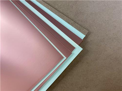
The image below shows the WL-CT615 hydrocarbon-ceramic fiberglass-clad copper laminate, displaying the copper-clad surface and the light-colored dielectric edge profile.
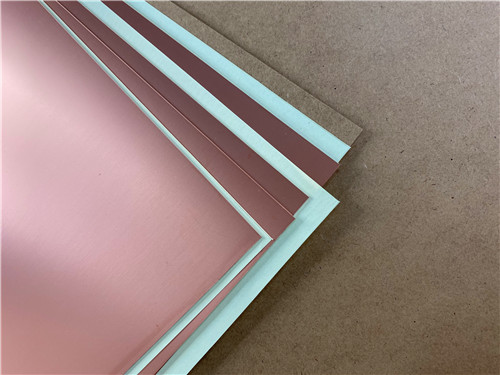
Figure 1. WL-CT615 hydrocarbon-ceramic fiberglass-clad copper laminate.
WL-CT615 is supplied exclusively with ED (electrodeposited) copper foil, available in standard thicknesses of 0.5 oz (0.018 mm) and 1 oz (0.035 mm). Other copper thicknesses are available by custom order. RTF (reverse treatment foil) copper — which offers superior PIM performance, reduced conductor loss, and lower insertion loss — is available for other WL-CT series grades but not for WL-CT615. RTF foil uses an adhesive backing that increases substrate thickness by 0.018 mm (0.7 mil) and provides excellent peel strength.
Standard panel sizes are 460 mm × 610 mm (18" × 24") and 915 mm × 1220 mm (36" × 48"). Custom sizes are available upon request.
The Wangling WL-CT series can be supplied with an aluminum backing (model designation WL-CT-AL), where one side of the dielectric is clad with copper and the other side is bonded to an aluminum base for electromagnetic shielding or enhanced heat dissipation. For example, WL-CT615-AL denotes the aluminum-backed version of WL-CT615. The aluminum base has a density of 2.7 g/cm³, thermal conductivity of 180 W/m·K, and CTE of 24 ppm/°C, with available thicknesses of 0.48, 0.98, 1.48, 1.98, 2.98, and 3.98 mm (other thicknesses by custom order).
• Aerospace and aviation equipment, space and cabin devices, aircraft
• Microwave circuits, antennas, and phase-sensitive antennas
• Early warning radar, airborne radar, and various radar systems
• Phased array antennas and beamforming networks
• Satellite communications and navigation systems
• Power amplifiers and high-frequency RF modules
The WL-CT615 copper-clad laminate is a high-Dk (6.15), low-loss (Df 0.004 at 10 GHz) hydrocarbon-ceramic thermosetting material that bridges the gap between expensive PTFE-based high-frequency laminates and standard FR-4. Its FR-4-like processability, high Tg (>280°C), copper-matched CTE (X: 15, Y: 17, Z: 33 ppm/°C), 0.72 W/m·K thermal conductivity, halogen-free formulation, and UL-94 V-0 flame retardancy make it a versatile and reliable choice for RF, microwave, radar, satellite, and aerospace applications.
Available in dielectric thicknesses from 8 mil upward with ED copper foil and in standard panel sizes, the WL-CT615 offers designers a domestically produced, cost-effective alternative to imported high-frequency laminates without compromising on electrical performance or thermal-mechanical reliability. Its radiation resistance and low outgassing further extend its suitability into space and high-altitude environments.
Previous:
Rogers 20mil AD250C PCB Pure Gold High-Frequency Antenna Circuit BoardNext:
High-Frequency 2-Layer PCB on 59mil Wangling TP440 Thermoplastic Dielectric Immersion GoldIf you have questions or suggestions,please leave us a message,we will reply you as soon as we can!
Categories
New Products
Wangling TP2200 PCB 0.8mm Substrate Immersion Gold 2-Layer High-Dk (Dk 22) RF Board
Rogers TMM10 PCB 5.08mm Core ENIG 2-Layer High-Dk Microwave Board
Taconic TLX-8 PCB 50mil ENIG 2-Layer High-Frequency RF Circuit Board
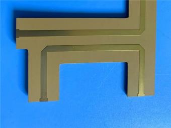
Wangling TF440 25mil DK4.4 Laminate Immersion Gold 2-Layer Copper-filling Vias PCB
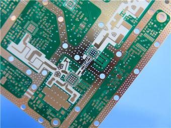
RO4360G2 Rogers 12mil ENEPIG 2-Layer DK6.15 High Frequency Custom PCB
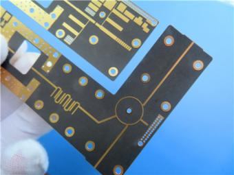
Wangling F4BTMS220 2-Layer DK2.2 PCB 10 mil Core with Immersion Gold
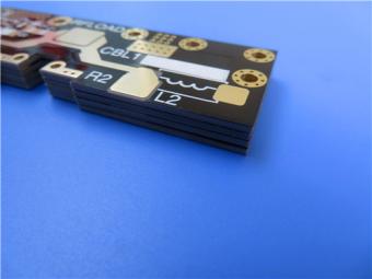
Wangling F4BTME350 10mil DK3.5 High Frequency Substrate PCB 2-Layer Immersion Gold
Wangling F4BTM300 Custom 2-layer PCB 20mil DK3.0 Substrate with Immersion Gold
Polytetrafluoroethylene (Short for PTFE), commonly known as "plastic king ", is a polymer compound made of tetrafluoroethylene by polymerization. It has excellent chemical stability, corrosion resistance, sealing, high lubrication and non-viscosity, electrical insulation and good aging resistance.
Rogers TMM4 thermoset microwave material is ceramic, hydrocarbon, thermoset polymer composite designed for high plated-through-hole reliability stripline and microstrip applications.
Taconic TLY laminates are a type of low loss laminates. They are manufactured with very light weight woven fiberglass and are more dimensionally stable than chopped fiber reinforced PTFE composites.
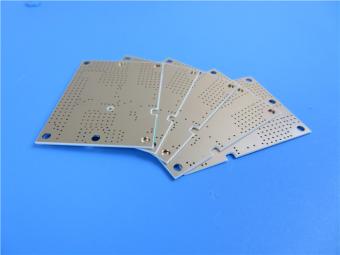
RO3203 laminates combine the surface smoothness of a non-woven PTFE laminate, for finer line etching tolerances, with the rigidity of a woven-glass PTFE laminate. These materials can be fabricated into printed circuit boards using
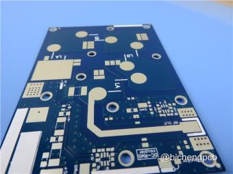
This type of immersion silver RF PCB is made on one of Taconic’s ORCER family material: RF-45.
Rogers’ TMM10 thermoset microwave materials are ceramic, hydrocarbon, thermoset polymer composites designed for high plated-thru-hole reliability stripline and microstrip applications.
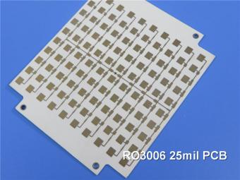
Rogers RO3006 was designed to offer exceptional electrical and mechanical stability at competitive prices.
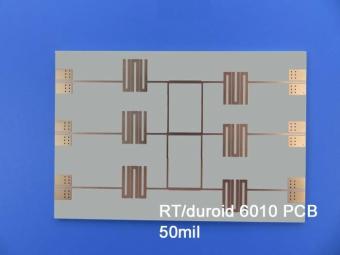
RT/duroid 6010LM microwave laminates feature ease of fabrication and stability in use. This property results in the possibility of mass production and reducing the cost of goods.
 6-11C Shidai Jingyuan, Fuyong, Baoan, Shenzhen, Guangdong, China 518103


For inquiries about our products or pricelist, please leave to us and we will be in touch within 24 hours.
© Copyright: 2026 Shenzhen Bicheng Electronics Technology Co., Ltd.. All Rights Reserved.

IPv6 network supported


