
 Call Us Now !
Tel : +86 755 27374946
Call Us Now !
Tel : +86 755 27374946
 Order Online Now !
Email : info@bichengpcb.com
Order Online Now !
Email : info@bichengpcb.com
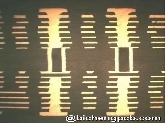
How to Distinguish the Step (Stack-up) of HDI PCB? Tag#Stacked via Staggered via HDI | PCB 1+N+1 HDI PCB | 2+N+2 HDI PCB HDI stands for high density interconnection. It contains non-mechanical drilling, the ring of microvias and blind via below 6 mil, internal and external layers of track width, track gap below 4 mil, pad diameter is not more than 0.35 mm. We call this kind of multi-layer PCB...
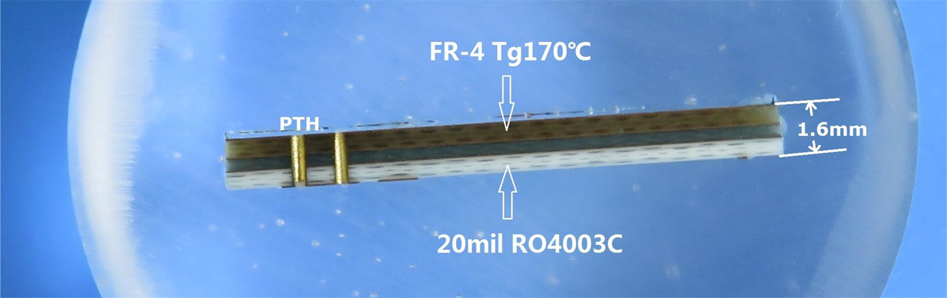
Multilayer Stackup Design: Minimizing Crosstalk in High-Speed PCBs Introduction In high-speed PCB design, signal integrity is paramount. As data rates increase, crosstalk—unwanted electromagnetic coupling between traces—becomes a critical challenge. A well-optimized multilayer stackup is essential to minimize crosstalk while ensuring signal integrity, power delivery, and manufacturability. This ar...
1
pagesCategories
New Blog
Tags
 6-11C Shidai Jingyuan, Fuyong, Baoan, Shenzhen, Guangdong, China 518103


For inquiries about our products or pricelist, please leave to us and we will be in touch within 24 hours.
© Copyright: 2026 Shenzhen Bicheng Electronics Technology Co., Ltd.. All Rights Reserved.

IPv6 network supported


