
 Call Us Now !
Tel : +86 755 27374946
Call Us Now !
Tel : +86 755 27374946
 Order Online Now !
Email : info@bichengpcb.com
Order Online Now !
Email : info@bichengpcb.com
What Makes WL-CT350 PCB the Right Material for Modern High-Frequency RF Designs?
What Makes WL-CT350 PCB the Right Material for Modern High-Frequency RF Designs?
Quick Answer
WL-CT350 PCB is a hydrocarbon-ceramic fiberglass-reinforced high-frequency circuit board material manufactured by Wangling. Designed as a thermosetting resin-based alternative to PTFE substrates, it delivers a dielectric constant of 3.48 and dissipation factor of 0.0039 at 10 GHz, combined with a Tg above 280°C and FR4-like processability. Its low TCDK (52 ppm/°C), closely copper-matched CTE, and 0.7 W/m·K thermal conductivity make it suitable for base station antennas, automotive radar, power amplifiers, and RF filters where signal stability and thermal reliability matter. Unlike PTFE materials, Wangling WL-CT350 can be fabricated using standard PCB manufacturing flows, reducing cost and lead time while maintaining consistent circuit performance.
Key Takeaways
- Low-loss high-frequency performance: Dk 3.48 and Df 0.0039 at 10 GHz support reliable signal transmission across RF and microwave bands.
- FR4-compatible manufacturing: Hydrocarbon-thermoset chemistry enables standard PCB processing, unlike PTFE which requires specialized fabrication techniques.
- Exceptional thermal stability: Tg > 280°C and TCDK of 52 ppm/°C ensure consistent electrical properties across wide temperature ranges.
- Copper-matched CTE: X-axis 11 ppm/°C and Y-axis 14 ppm/°C minimize thermal stress on traces and plated vias, improving long-term reliability.
- Enhanced thermal management: Thermal conductivity of 0.7 W/m·K—roughly double standard FR4—aids heat dissipation in power-dense RF designs.
- Low moisture absorption: 0.05% absorption rate preserves impedance stability in high-humidity outdoor environments.
- Domestic import substitute: Cost-effective alternative to imported high-frequency laminates with comparable electrical specifications.
---
Understanding WL-CT350: A High-Frequency Substrate Built for Manufacturability
When selecting materials for RF and microwave circuits, engineers traditionally face a tradeoff: premium PTFE-based substrates deliver excellent electrical performance but are expensive and difficult to manufacture, while standard FR4 is cheap and processable but loses signal integrity at higher frequencies. WL-CT350, developed by Wangling, addresses this gap through a carefully engineered hydrocarbon-ceramic composite that combines strong high-frequency characteristics with FR4-like fabrication compatibility.
Material Composition and Architecture
WL-CT350 substrate is classified as an organic polymer ceramic fiberglass cloth copper clad laminate (CCL). Its dielectric layer is built from three core constituents:
1. Hydrocarbon resin matrix—A thermosetting polymer system that forms the structural binder of the material. Unlike PTFE (a thermoplastic), hydrocarbon resins cure into a rigid, dimensionally stable structure that behaves predictably during standard PCB manufacturing operations.
2. Ceramic filler particles—Dispersed throughout the resin matrix, ceramic fillers precisely tune the dielectric constant, boost thermal conductivity, and improve the temperature stability of both Dk and Df.
3. Woven fiberglass reinforcement—Provides mechanical strength and dimensional stability, functioning the same way it does in conventional FR4 substrates.
This three-part formulation is what gives WL-CT350 its dual advantage: the hydrocarbon-ceramic blend delivers the low-loss electrical performance needed for high-frequency designs, while the fiberglass-reinforced thermoset structure preserves the manufacturability that PCB fabricators rely on.
Electrical Performance: Dk, Df, and Why They Matter
Thermal and Mechanical Reliability Characteristics
- X-axis: 11 ppm/°C
- Y-axis: 14 ppm/°C
- Z-axis: 34 ppm/°C
Moisture Resistance for Outdoor Deployments
---
Practical Implementation: 2-Layer WL-CT350 Stackup and Manufacturing
A typical2-layer WL-CT350 PCB configuration illustrates how the material translates into real-world designs. The standard stackup is straightforward:
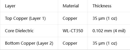
This 2-layer rigid configuration is commonly used for antenna feed networks, simple filter boards, and RF transmission line structures where controlled impedance microstrip lines are routed on the top layer with a solid ground plane on the bottom.
Manufacturing Advantages Over PTFE
The manufacturability of WL-CT350 is one of its most significant differentiators from PTFE-based materials:
1) Drilling:
WL-CT350 drills cleanly with standard carbide tooling, producing well-defined hole walls with minimal burring. PTFE materials, by contrast, are soft and prone to smearing during drilling, often requiring specialized drill parameters and additional desmear or plasma etch steps to achieve reliable hole wall preparation for plating.
2) Plating and metallization:
The hydrocarbon resin surface accepts standard electroless copper deposition processes without special surface treatment, which is not the case for PTFE—PTFE's low surface energy typically requires sodium naphthalene etching or plasma treatment to achieve adequate copper adhesion.
3) Lamination and multilayer processing:
As a thermosetting material, WL-CT350 laminates predictably with matching prepreg materials, following lamination profiles similar to FR4. PTFE materials often require more complex lamination cycles with tighter pressure and temperature controls.
4) Dimensional stability:
The fiberglass reinforcement provides excellent dimensional stability during fabrication, ensuring that trace geometries and board dimensions remain consistent across production panels—an important factor for impedance-controlled RF boards.
Production files for WL-CT350 PCBs are supplied in standard Gerber RS-274-X format, and finished boards are typically inspected and tested to IPC-Class-2 acceptance standards, with 100% electrical testing performed before shipment. This adherence to industry-standard formats and specifications makes WL-CT350 easy to integrate into existing PCB procurement and quality assurance workflows.
---
Typical Application Areas
WL-CT350's combination of electrical performance, thermal stability, and manufacturing practicality makes it suitable for a broad range of high-frequency applications:
1) Base Station Antennas and Satellite Antennas—5G massive MIMO arrays and satellite communication antennas require consistent element-to-element performance across temperature extremes. WL-CT350's stable Dk and low loss ensure that each radiating element maintains its designed impedance and radiation characteristics.
2) Automotive Radar, Sensors, and Navigation Systems—Automotive radar modules (24 GHz and 77 GHz bands) must operate reliably from−40°C to +125°C while subjected to vibration and thermal cycling. The material's high Tg, matched CTE, and low TCDK align well with automotive reliability requirements.
3) Power Amplifiers—RF power amplifiers generate significant heat and benefit from WL-CT350's 0.7 W/m·K thermal conductivity. Stable Dk also ensures that impedance matching networks remain effective as the board temperature rises under load.
4) Satellite High-Frequency Heads (LNBs)—Low-noise block downconverters demand low-loss substrates at Ku-band frequencies. WL-CT350's low dissipation factor directly contributes to better system noise figure and reception sensitivity.
5) RF Devices and Filters—Filters and duplexers are highly sensitive to Dk variations. The 52 ppm/°C TCDK of WL-CT350 helps filter designs maintain their passband characteristics across operating temperature ranges.
6) WiMAX Antennas and Distributed Antenna Systems (DAS)—These infrastructure applications require cost-effective, volume-manufacturable substrates with consistent RF performance. WL-CT350's FR4-like processability supports high-volume production at a lower cost than PTFE alternatives.
---
Frequently Asked Questions (FAQ)
1) How does WL-CT350 compare to PTFE-based high-frequency substrates?
WL-CT350 generally has slightly higher loss than premium PTFE-ceramic materials but offers significantly better manufacturability and cost efficiency. PTFE substrates require specialized drilling, plasma surface treatment, and controlled lamination processes, all of which increase production cost and lead time. WL-CT350 processes with standard FR4-compatible workflows while still delivering strong high-frequency performance for most commercial RF applications.
2) Can WL-CT350 be used in multilayer PCB designs?
Yes. While the reference configuration in this article is a 2-layer stackup, WL-CT350 is available as a core material and can be used in multilayer constructions with compatible prepreg materials. It supports plated through-holes and can be integrated into mixed-dielectric stackups when combined with other material types.
3) Up to what frequency can WL-CT350 be used effectively?
WL-CT350 is characterized at 10 GHz and performs well through commonly used microwave bands including those for 5G sub-6 GHz, 24 GHz and 77 GHz automotive radar, and Ku-band satellite communications. Usability at higher frequencies depends on the specific design's loss budget and performance requirements.
4) Is WL-CT350 compatible with lead-free soldering processes?
Yes. With a Tg above 280°C, WL-CT350 comfortably withstands standard lead-free reflow profiles with peak temperatures around 250–260°C. The material is formulated to meet modern RoHS requirements and supports all common surface finishes including ENIG, lead-free HASL, OSP, and immersion silver.
5) What are the cost implications of choosing WL-CT350 versus imported alternatives?
WL-CT350 is positioned as a cost-competitive domestic alternative to imported high-frequency laminates. While pricing varies with volume, copper weight, and panel size, it typically provides meaningful cost savings compared to premium imported PTFE or hydrocarbon-ceramic materials, with comparable electrical performance for many commercial and industrial RF applications.
6) Does WL-CT350 require special storage or handling?
Standard PCB material storage practices apply—controlled temperature and humidity environments are recommended to prevent moisture uptake prior to fabrication. WL-CT350's low inherent moisture absorption rate (0.05%) makes it less sensitive to ambient conditions than some other high-frequency substrate materials.
---
Conclusion
WL-CT350 occupies a valuable position in the high-frequency PCB material landscape: it delivers the low-loss electrical performance and thermal stability that modern RF designs demand, while retaining the manufacturing simplicity and cost structure of conventional FR4-compatible materials. For engineers working on base station antennas, automotive radar, power amplifiers, filters, or satellite front-ends, it offers a practical balance of performance, reliability, and producibility.
As a domestically developed hydrocarbon-ceramic composite with well-characterized specifications and IPC-Class-2 compliance, WL-CT350 also provides supply chain resilience as a substitute for imported high-frequency laminates. Its combination of proven electrical data, thermal robustness, and manufacturing compatibility makes it a strong candidate for a wide range of current and next-generation RF and microwave PCB designs.
Categories
New Blog
Tags
 6-11C Shidai Jingyuan, Fuyong, Baoan, Shenzhen, Guangdong, China 518103


For inquiries about our products or pricelist, please leave to us and we will be in touch within 24 hours.
© Copyright: 2026 Shenzhen Bicheng Electronics Technology Co., Ltd.. All Rights Reserved.

IPv6 network supported


