

 Call Us Now !
Tel : +86 755 27374946
Call Us Now !
Tel : +86 755 27374946
 Order Online Now !
Email : info@bichengpcb.com
Order Online Now !
Email : info@bichengpcb.com
Microwave composite dielectric copper-clad laminate-TP
Item NO.:
BIC-231-v296.0Order(MOQ):
1-10Payment:
T/TProduct Origin:
ChinaShipping Port:
ShenzhenLead Time:
7-10 days
TP High Frequency1.5mm Material PCB Microwave Composite Dielectric Copper-clad Laminate
Introduction
TP material is a unique high-frequency thermoplastic material in the industry. The dielectric layer of TP-type laminates consists of ceramics and polyphenylene Oxide resin (PPO), without fiberglass reinforcement. The dielectric constant can be precisely adjusted by adjusting the ratio between ceramics and PPO resin. The production process is special, and it has excellent dielectric performance and high reliability. TP refers to the smooth surface material without copper cladding, TP-1 refers to the material with copper cladding on one side, and TP-2 refers to the material with copper cladding on both sides.
Features
1. The dielectric constant can be arbitrarily selected within the range of 3 to 25 according to circuit requirements, and it is stable. Common dielectric constants include 3.0, 4.4, 6.0, 6.15, 9.2, 9.6, 10.2, 11, 16, and 20. The dielectric loss islow, and the loss increases as the frequency increases, but the change is not significant within 10 GHz.
2. Long-term operating temperature ranges from -100°C to +150°C. It has excellent low-temperature resistance. When the temperature exceeds 180°C, the material may deform, the copper foil may peel off, and there may be significant changes in electrical performance.
3. The thinnest thickness is 0.5mm, and it is available in various thicknesses and can be customized.
4. It is resistant to radiation and has low outgassing.
5. Ideal material for Beidou, missile-borne, fuze, and miniaturized antennas.
6. The adhesion between copper foil and dielectric is more reliable than ceramic substrates with vacuum coating. The material is easy to machine and can be processed through drilling, turning, grinding, shearing, etching, and other methods, which ceramic substrates cannot achieve.
7. Convenient for PCB processing, it can be processed using methods suitable for thermoplastic materials, resulting in high yield and reduced processing cost compared to ceramic substrates. Due to the characteristics of the material, it is generally not recommended for multilayer PCB processing. If multilayer PCB processing is required, low-temperature bonding sheets should be selected, and feasibility should be fully considered.
Data Sheet
| Product Technical Parameter | Product Models & Data Sheet | |||||||||||||||
| Product Features | Test Conditions | Unit | TP TP-1 TP-2 | |||||||||||||
| Dielectric Constant |
When the dielectric constant is ≤11, the test condition is 10GHz. When the dielectric constant is >11, the test condition is 5GHz. |
/ | 3.0±0.06 | 4.4±0.09 | 6.0±0.12 | |||||||||||
| 6.15±0.12 | 9.2±0.18 | 9.6±0.19 | ||||||||||||||
| 10.2±0.2 | 11.0±0.022 | 16.0±0.4 | ||||||||||||||
| 20.0±0.8 | 22.0±0.88 | 25.0±1.0 | ||||||||||||||
| The dielectric constant can be customized within the range of 3.0 to 25. | ||||||||||||||||
| Dielectric Constant Tolerance | Dielectric Constant 3.0~11.0 | / | ±2% | |||||||||||||
| Dielectric Constant 11.1~16.0 | / | ±2.5% | ||||||||||||||
| Dielectric Constant 16.1~25.0 | / | ±4% | ||||||||||||||
| Loss Tangent | Loss Tangent 3.0~9.5 | 10GHz | / | 0.0010 | ||||||||||||
| Loss Tangent 9.6~11.0 | 10GHz | / | 0.0012 | |||||||||||||
| Loss Tangent 11.1~16.0 | 5GHz | / | 0.0015 | |||||||||||||
| Loss Tangent 16.1~25.0 | 5GHz | / | 0.0020~0.0025 | |||||||||||||
| Dielectric Constant Temperature Coefficient | Dielectric Constant 3.0~9.5 | -55 º~150ºC | PPM/℃ | -50 | ||||||||||||
| Dielectric Constant 9.6~16.0 | -55 º~150ºC | PPM/℃ | -40 | |||||||||||||
| Dielectric Constant 16.1~25.0 | -55 º~150ºC | PPM/℃ | -55 | |||||||||||||
| Peel Strength | 1 OZ Normal State | N/mm | >0.6 | |||||||||||||
| 1 OZ After AC Humidity Test | N/mm | >0.4 | ||||||||||||||
| Volume Resistivity | Normal State at 500V | MΩ.cm | >1×10⁹ | |||||||||||||
| Surface Resistivity | Normal State at 500V | MΩ | >1×10⁷ | |||||||||||||
|
Coefficient of Thermal Expansion (XY Z) |
Dielectric Constant 3.00~4.40 | -55 º~150ºC | PPM/℃ | 60,60,70 | ||||||||||||
| Dielectric Constant 4.60~6.15 | -55 º~150ºC | PPM/℃ | 50,50,60 | |||||||||||||
| Dielectric Constant 6.16~11.0 | -55 º~150ºC | PPM/℃ | 40,40,55 | |||||||||||||
| Dielectric Constant 11.1~16.0 | -55 º~150ºC | PPM/℃ | 40,40,50 | |||||||||||||
| Dielectric Constant 16.1~25.0 | -55 º~150ºC | PPM/℃ | 35,35,40 | |||||||||||||
| Water Absorption | 20±2℃, 24 hours | % | ≤0.01 | |||||||||||||
| Long-Term Operating Temperature | High-Low Temperature Chamber | ℃ | -100º~150ºC | |||||||||||||
| Material Composition | Polyphenylene ether, ceramic, paired with ED copper foil. | |||||||||||||||
| The density and thermal conductivity data for materials with different dielectric constants are as follows: | ||||||||||||||||
| Product Features | Unit | Dielectric Constanct | ||||||||||||||
| 3.0 | 4.4 | 6.0 | 6.15 | 9.6 | 10.2 | 11.0 | 16.0 | 20.0 | 22.0 | 25.0 | ||||||
| Density | g/cm3 | 1.69 | 1.89 | 2.1 | 2.12 | 2.26 | 2.33 | 2.40 | 2.76 | 2.73 | 2.77 | 2.94 | ||||
| Thermal Conductivity | W/(M.K) | 0.40 | 0.44 | 0.55 | 0.55 | 0.65 | 0.67 | 0.70 | 0.80 | 0.85 | 0.90 | 1.0 | ||||
Our PCB Capability (TP Series)
| PCB Capability (TP Series) | |||
| PCB Material: | Polyphenylene ether, ceramic | ||
| Designation (TP Series) | Designation | DK | DF |
| TP300 | 3.0±0.06 | 0.0010 | |
| TP440 | 4.4±0.09 | 0.0010 | |
| TP600 | 6.0±0.12 | 0.0010 | |
| TP615 | 6.15±0.12 | 0.0010 | |
| TP920 | 9.2±0.18 | 0.0010 | |
| TP960 | 9.6±0.2 | 0.0011 | |
| TP1020 | 10.2±0.2 | 0.0011 | |
| TP1100 | 11.0±0.22 | 0.0011 | |
| TP1600 | 16.0±0.32 | 0.0015 | |
| TP2000 | 20.0±0.4 | 0.0020 | |
| TP2200 | 22.0±0.44 | 0.0022 | |
| TP2500 | 25.0±0.5 | 0.0025 | |
| Layer count: | Single Sided, Double Sided PCB | ||
| Copper weight: | 1oz (35µm), 2oz (70µm) | ||
| Dielectric thickness (Dielectric thickness or overall thickness) | 0.5mm, 0.8mm, 1.0mm, 1.2mm, 1.5mm, 2.0mm, 3.0mm, 4.0mm, 5.0mm, 6.0mm, 7.0mm, 8.0mm, 10.0mm, 12.0mm | ||
| PCB size: | ≤150mm X 220mm | ||
| Solder mask: | Green, Black, Blue, Yellow, Red etc. | ||
| Surface finish: | Bare copper, HASL, ENIG, Immersion silver, Immersion tin, OSP, Pure gold, ENEPIG etc.. | ||
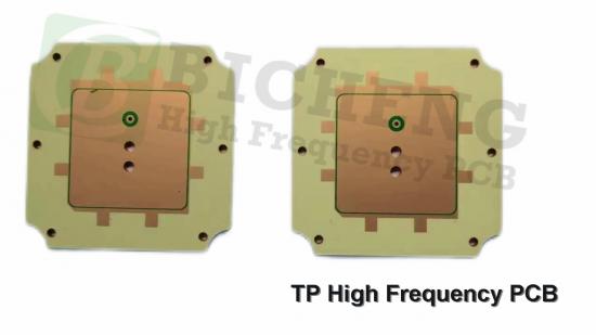
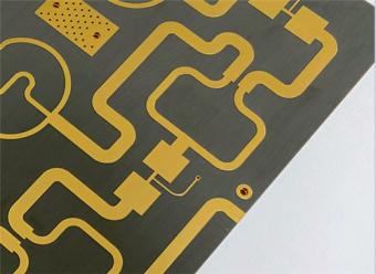
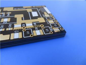
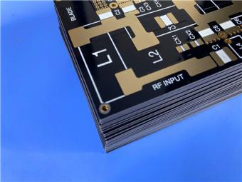
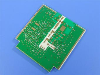
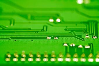
A TP PCB and Applications
On the screen, you can see a 1.5mm TP high-frequency PCB with OSP (Organic Solderability Preservative) coating. TP high-frequency PCBs are also utilized in applications such as Beidou, missile-borne systems, fuzes, and miniaturized antennas.

Final Attention
The material is not suitable for 260°C thermal shock testing and cannot be wave soldered. Hand soldering with a constant temperature soldering iron is recommended. Reflow soldering is generally not recommended. If reflow soldering is carried out, the highest set temperature should not exceed 200°C, and feasibility and stability should be fully considered.


Previous:
F4BTM High Frequency PCB DK 3.0 F4BTM 1.524mm Substrate HASL Surface FinishesNext:
F4BME Series Laminates High Frequency Aluminum-based PCB F4BME225If you have questions or suggestions,please leave us a message,we will reply you as soon as we can!
Categories
New Products
Wangling 5mil 0.127mm TFA300 Core 2-layer Immersion Gold Green Solder Mask PCB
7.5mil AGC Taconic TLY-5 Substrate Custom PCB EPIG Finish Bare Copper
10mil Rogers CuClad 250 Immersion Gold 2-Layer Rigid Microwave PCB
20mil F4BTMS450 Wangling DK4.5 Laminate Custom PCB HASL LF Finsh
F4BME275 Wangling DK2.75 Laminate 2-Layer 1.6mm Pure Gold RF Custom PCB
Wangling F4BTD350S High Frequency PCB 2-layer 20mil Thick ENIG DK3.5 Substrate
12-layer TG200 TU-872 SLK High-Speed FR4 1.68mm PCB with ENIG Impedance Control
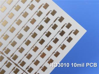
12-Layer RO4350B + RO3010 3.14mm Hybrid PCB Nickel-Free EPIG Surface Finish Blind Via

RF-10 25mil Taconic PCB Materials stands out as a high-performance solution for RF applications. Its exceptional electrical properties, dimensional stability, thermal conductivity, and adhesion characteristics make it an ideal choice for demanding applications.
The PCB has a 4-layer hybrid stackup with a 0.5oz+plating ground layer, two 1oz ground layers, and a 0.5oz+plating signal layer.
The dimensions of the board are 55.00 x 26.00 mm, with a tolerance of +/- 0.15mm. The board has 16 components, 26 total pads, 9 through-hole pads, 10 top SMT pads, 7 bottom SMT pads, 77 vias, and 82 nets.
Rogers RO4003C PCB is an innovative and advanced circuit board that is made with high-quality materials.
The RO4350B PCB offers a range of benefits that make it an ideal choice for high-frequency applications. Its low dielectric loss and high thermal conductivity make it perfect for high-frequency applications such as RF and microwave circuits.
Bicheng PCB Ships High-Quality PCBs with Shengyi Tg150 ℃ S1000H Material and Advanced Stackup
Rogers RO3010 PCB is ideal for a wide range of high-frequency applications, including power amplifiers, filters, couplers, and antennas.
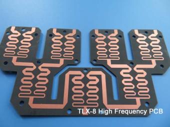
TLX-8 features low dielectric loss, low moisture absorption, and excellent thermal stability, making it ideal for high-frequency and high-speed applications. It has a low dissipation factor, which helps to minimize signal loss and distortion.
 6-11C Shidai Jingyuan, Fuyong, Baoan, Shenzhen, Guangdong, China 518103


For inquiries about our products or pricelist, please leave to us and we will be in touch within 24 hours.
© Copyright: 2026 Shenzhen Bicheng Electronics Technology Co., Ltd.. All Rights Reserved.

IPv6 network supported


