

 Call Us Now !
Tel : +86 755 27374946
Call Us Now !
Tel : +86 755 27374946
 Order Online Now !
Email : info@bichengpcb.com
Order Online Now !
Email : info@bichengpcb.com
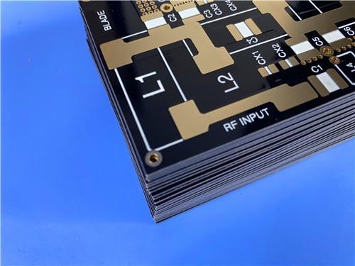
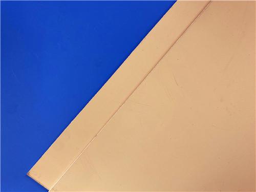
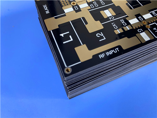
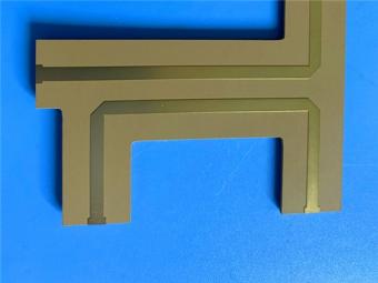
The F4BTD350S 2-layer ENIG PCB is a thermally enhanced, low-loss high-frequency circuit board that bridges the gap between cost-sensitive FR-4 designs and premium high-end PTFE boards.
Item NO.:
BIC-593-v678.0Order(MOQ):
1-10Payment:
T/TProduct Origin:
ChinaShipping Port:
ShenzhenLead Time:
7-10 days
Wangling F4BTD350S High Frequency PCB 2-layer 20mil Thick ENIG DK3.5 Substrate
Executive Summary
Thispage presents a comprehensive technical overview of the F4BTD350S 2-layer printed circuit board, a 0.6 mm-thick high-frequency PCB built on Wangling F4BTD350S PTFE ceramic-filled substrate with electroless nickel immersion gold (ENIG) surface finish. Engineered for high-power RF and microwave applications requiring both low insertion loss and efficient heat dissipation, this 79×110 mm double-sided board combines a Dk of 3.5 at 10 GHz, a dissipation factor of 0.0016, and a through-plane thermal conductivity of 1.25 W/m·K—a combination that distinguishes it from standard FR-4 and even conventional PTFE boards. Manufactured to IPC-Class-2 quality standards with 100% electrical testing prior to shipment, the board supports 7/9 mil trace/space geometries, 0.6 mm minimum through-holes, and 1 oz finished copper on both outer layers.
The following description is structured in two independent sections: the first covers the 20mil F4BTD350S PCB product itself, including construction, stackup, and board-level statistics; the second provides an in-depth datasheet-level examination of the F4BTD350S copper-clad laminate (CCL) material. Both sections conclude separately to preserve logical separation and avoid content duplication.
Part 1: F4BTD350S 2-Layer PCB Product Description
1.1 PCB Construction Details
The table below summarizes the core construction parameters of this F4BTD350S PCB, covering base material, geometry, copper weight, surface finish, and quality control attributes.
|
Parameter |
Specification |
|
Base Material |
F4BTD350S |
|
Layer Count |
2 layers (double-sided, rigid) |
|
Board Dimensions |
79 mm × 110 mm, ±0.15 mm tolerance |
|
Finished Board Thickness |
0.6 mm (20 mil) |
|
Finished Copper Weight |
1 oz (35 μm / 1.4 mil) on both outer layers |
|
Minimum Trace / Space |
7 mil / 9 mil |
|
Minimum Hole Size |
0.6 mm (through-hole only; no blind vias) |
|
Via Plating Thickness |
≥ 20 μm |
|
Surface Finish |
Immersion Gold (ENIG) |
|
Top Solder Mask |
Black |
|
Bottom Solder Mask |
None |
|
Top Silkscreen |
White |
|
Bottom Silkscreen |
None |
|
Electrical Test |
100% tested before shipment |
|
Quality Standard |
IPC-Class-2 |
|
Artwork Format |
Gerber RS-274-X |
|
Availability |
Worldwide |
1.2 PCB Stackup Configuration
This 2-layer rigid PCB uses a symmetric core-only stackup with identical 35μm copper foils on both sides of a 0.508 mm F4BTD350S dielectric core. The summary table below presents the layer-by-layer build.
|
Layer |
Material |
Thickness |
|
Layer 1 (Top) |
Copper |
35 μm (1 oz) |
|
Core Dielectric |
F4BTD350S |
0.508 mm (20 mil) |
|
Layer 2 (Bottom) |
Copper |
35 μm (1 oz) |
1.3 PCB Board Statistics
The following table quantifies the component, pad, via, and net count on this specific board design, providing a quick reference for assembly complexity and routing density.
|
Metric |
Count |
|
Total Components |
18 |
|
Total Pads |
22 |
|
Through-Hole Pads |
10 |
|
Top-Side SMT Pads |
12 |
|
Bottom-Side SMT Pads |
0 |
|
Vias |
6 |
|
Nets |
2 |
1.4. Key Differentiators
The F4BTD350S PCB delivers several differentiated performance characteristics that set it apart from conventional FR-4 and standard high-frequency boards. First and foremost is the exceptional thermal conductivity of 1.25 W/(m·K)—approximately 3–4 times higher than standard FR-4 materials (typically 0.3–0.4 W/(m·K))—enabling efficient heat dissipation from high-power RF components such as power amplifiers and industrial heating elements. This thermal advantage directly translates to higher power handling capability and extended component lifespan.
Second, the material exhibits ultra-low dielectric loss with a dissipation factor of only 0.0016 at 10GHz, ensuring minimal signal attenuation even at microwave frequencies. Combined with a tightly controlled dielectric constant of 3.5±0.07 and a low thermal coefficient of Dk at -45 ppm/°C, the board maintains consistent impedance characteristics across wide operating temperature ranges from -55°C to 150°C—critical for maintaining filter and coupler performance in demanding environments.
Third, the ENIG surface finish provides a flat, solderable surface with excellent shelf life and wire-bonding capability, making it suitable for high-frequency applications where surface roughness directly impacts signal propagation. The 20μm via plating thickness ensures reliable through-hole interconnects with low resistance, while the IPC-Class-2 manufacturing standard guarantees consistent quality and dimensional accuracy.
1.5 Application Suitability
This Wangling PCB is particularly suited for the following applications:
1)High-Power RF Circuits: The combination of low-loss F4BTD350S (Df: 0.0016 at 10GHz) with high thermal conductivity (1.25W/(M·K)) enables sustained power handling without exceeding component temperature limits.
2)Power Amplifiers: The 0.6mm thickness reduces parasitic inductance in ground planes, improving amplifier stability at UHF and microwave frequencies.
3)Antenna Feed Networks: The tight Dk tolerance of±0.07 ensures consistent phase and amplitude balance in beam-forming networks and corporate feed structures.
4)Industrial Heating Equipment: The -55°C to +260°C operating range and high electric strength (25KV/mm) make this board viable for industrial RF heating applications at elevated temperatures.
5)Couplers and Filters: The low-loss characteristic (Df: 0.0016) minimizes inserted loss in coupled-line directional couplers and microstrip filters, preserving system sensitivity and dynamic range.
PCB Conclusion
In summary, the F4BTD350S 2-layer ENIG PCB is a thermally enhanced, low-loss high-frequency circuit board that bridges the gap between cost-sensitive FR-4 designs and premium high-end PTFE boards. Its 0.6 mm core-only stackup, 1 oz copper, 7/9 mil trace capability, and ENIG surface finish provide a manufacturable, assembly-friendly platform, while the underlying F4BTD350S substrate delivers 1.25 W/m·K thermal conductivity and 0.0016 @ 10 GHz loss performance that standard materials cannot match. With IPC-Class-2 quality, 100% electrical testing, and worldwide availability, this board is a practical choice for engineers designing high-power RF, microwave, and industrial heating systems who need better thermal management and lower loss than FR-4 without stepping into the price tier of exotic aerospace-grade laminates.
Part 2: F4BTD350S Copper-Clad Laminate (CCL)—In-Depth Material Datasheet
2.1 Material Introduction
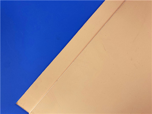
F4BTD350S is a high thermal conductivity PTFE resin-based high-frequency substrate, reinforced with glass fiber cloth and incorporating a high loading of thermally conductive specialty ceramics. This advanced composition delivers an exceptional combination of low dielectric loss and high thermal conductivity, positioning it as a next-generation material solution for applications demanding low insertion loss and efficient heat dissipation. It serves as a direct replacement for comparable imported high-frequency laminates.
The material's low loss and superior thermal conductivity enhance microwave power tolerance, extend device operational life, and enable reliable performance in high-temperature and long-duration service conditions. The benefits extend beyond thermal and electrical performance to include low coefficient of thermal expansion, excellent dimensional stability, high electrical strength, and high insulation resistance—facilitating easier PCB processing, higher through-hole reliability, lower soldering defects, improved component compatibility, and greater environmental adaptability.
The F4BTD350S laminate can be processed using standard PTFE sheet processing techniques. Its mechanical and physical properties make it suitable for multilayer, high-multilayer, and backplane applications, with excellent processability for dense-hole and fine-line designs.
2.2 F4BTD350S Product Features
|
Feature |
Description |
|
High Thermal Conductivity |
1.25W/(M·K)—approximately 3× higher than standard PTFE materials |
|
Low Loss |
Dissipation factor of 0.0016 at 10GHz |
|
High Power Tolerance |
Superior heat dissipation extends device life |
|
High Reliability |
Stable performance across temperature extremes |
|
Stable Dielectric Constant with Temperature |
-45 ppm/°C thermal coefficient of Dk (-55°C to 150°C) |
|
Low CTE and Dimensional Stability |
X-axis 11 ppm/°C, Y-axis 10 ppm/°C (-55°C to 288°C) |
|
Radiation Resistance |
Suitable for aerospace and other radiation-exposed environments |
|
Low Outgassing |
Compliant with vacuum system requirements |
|
Low Water Absorption |
≤0.05% (24-hour immersion) |
2.3 Complete F4BTD350S Datasheet Table
The following table consolidates the full set of electrical, thermal, mechanical, and environmental properties of the F4BTD350S CCL material.
|
Product Characteristic |
Test Condition |
Unit |
F4BTD350S Value |
|
Dielectric Constant (Typical) |
2GHz |
— |
3.52 |
|
Dielectric Constant (Typical) |
10GHz |
— |
3.5 |
|
Dielectric Constant Tolerance |
— |
— |
±0.07 |
|
Dielectric Constant (Design Value) |
10GHz |
— |
3.62 |
|
Loss Factor (Typical) |
2GHz |
— |
0.0012 |
|
Loss Factor (Typical) |
10GHz |
— |
0.0016 |
|
Dielectric Constant Temperature Coefficient |
-55°C to 150°C |
ppm/°C |
-45 |
|
Peel Strength (1oz Copper Foil) |
— |
N/mm |
>0.8 |
|
Volume Resistivity |
C96/23/95 |
MΩ·cm |
1×10¹¹ |
|
Surface Resistance |
C96/23/95 |
MΩ |
1×10¹² |
|
Electric Strength (Z-Direction) |
5KW, 500V/s |
KV/mm |
25 |
|
Breakdown Voltage (Horizontal) |
5KW, 500V/s |
KV |
38 |
|
Relative Tracking Index (CTI) |
23°C/50%/24H |
V |
600 |
|
CTE (X, Y Direction) |
-55°C to 288°C |
ppm/°C |
11, 10 |
|
CTE (Z Direction) |
-55°C to 288°C |
ppm/°C |
40 |
|
Thermal Decomposition Temperature (Td) |
5% Mass Loss |
°C |
500 |
|
Flexural Strength (X, Y Direction) |
Normal State |
MPa |
74, 64 |
|
Tensile Strength (X, Y Direction) |
Normal State |
MPa |
48, 45 |
|
Flexural Modulus (X, Y Direction) |
Normal State |
MPa |
7500, 7000 |
|
Dimensional Stability (X, Y Direction) |
After Etching and Baking |
% |
0.08, 0.18 |
|
Thermal Stress (260°C/10s/3 times) |
— |
— |
No Delamination |
|
Thermal Conductivity |
Z-Direction |
W/(M·K) |
1.25 |
|
Specific Heat Capacity |
— |
J/(g·°C) |
0.8 |
|
Density |
Normal Temperature |
g/cm³ |
2.21 |
|
Long-Term Service Temperature |
High/Low Temperature Chamber |
°C |
-55 to +260 |
|
Water Absorption |
20±2°C, 24 Hours |
% |
≤0.05 |
|
Flame Retardancy |
— |
UL-94 |
V-0 |
|
Dielectric Layer Composition |
— |
— |
PTFE + Glass Fiber Cloth + High Thermal Conductivity Ceramics |
Test methods follow or reference IPC-TM-650, GB/T 12636-1990 (stripline method for Dk/Df), and GB/T 4722-2017. All values are typical measurements provided for material selection reference.
2.4 Optional Configurations
|
Parameter |
Options |
|
Standard Copper Foil Thickness |
0.5 oz (0.018mm), 1 oz (0.035mm) |
|
Copper Foil Type |
Standard RTF Low-Roughness Copper Foil |
|
Alternative Substrates |
Aluminum Base, Copper Base (available upon request) |
|
Standard Sizes |
305×460mm (12"×18"), 460×610mm (18"×24") |
2.5 Dielectric Layer Thickness Availability
|
Dielectric Thickness |
Tolerance |
|
0.127mm (5mil) |
±0.0127mm (0.5mil) |
|
0.254mm (10mil) |
±0.02mm (1.0mil) |
|
0.508mm (20mil) |
±0.03mm (1.19mil) |
|
0.635mm (25mil) |
±0.04mm (1.58mil) |
|
0.762mm (30mil) |
±0.04mm (1.58mil) |
|
1.016mm (40mil) |
±0.05mm (2.0mil) |
|
1.270mm (50mil) |
±0.05mm (2.0mil) |
|
1.524mm (60mil) |
±0.06mm (2.5mil) |
|
2.03mm (80mil) |
±0.08mm (3.2mil) |
|
2.54mm (100mil) |
±0.10mm (4.0mil) |
|
3.175mm (125mil) |
±0.13mm (5.0mil) |
|
4.06mm (160mil) |
±0.18mm (7.0mil) |
|
5.08mm (200mil) |
±0.20mm (8.0mil) |
|
6.35mm (250mil) |
±0.25mm (10mil) |
2.6 F4BTD Series Aluminum/Copper Clad Substrates
Aluminum- or copper-clad variants are available where one side of the dielectric layer is bonded to a copper foil and the other side to a copper or aluminum base plate for shielding or heat dissipation purposes:
|
Model |
Metal Cladding |
Density (g/cm³) |
Thermal Conductivity (W/(M·K)) |
CTE (ppm/°C) |
Available Metal Base Thicknesses (mm) |
Available Sizes (mm) |
|
F4BTD*-CU |
Copper/Brass |
8.9 |
380 |
17 |
0.48, 0.98, 1.48, 1.98, 2.98, 3.98 |
460×610, 460×305 |
|
F4BTD*-AL |
Aluminum |
2.7 |
180 |
24 |
0.48, 0.98, 1.48, 1.98, 2.98, 3.98 |
460×610, 460×305 |
2.7 CCL Conclusion
F4BTD350S is a well-balanced high-thermal-conductivity PTFE-glass-ceramic laminate that addresses a real market need: microwave and RF power applications that require better thermal management than standard PTFE boards but cannot justify the cost or processing complexity of ceramic or metal-core substrates. With a Dk of 3.50±0.07, Df of 0.0016 at 10 GHz, and thermal conductivity of 1.25 W/m·K, backed by strong mechanicals, low CTE, 500°C Td, UL-94 V-0, and 600 V CTI, the material covers the electrical, thermal, safety, and reliability bases required by high-power RF, power amplifier, antenna, and industrial heating designs. Its compatibility with standard PTFE PCB processing and its availability in multiple copper weights, panel sizes, and dielectric thicknesses make it a flexible and manufacturable choice for both prototype and volume production. When paired with a well-designed 2-layer stackup and ENIG surface finish—as in the PCB described in Part 1—F4BTD350S delivers a compelling combination of performance, reliability, and practicality.
Previous:
F4BME275 Wangling DK2.75 Laminate 2-Layer 1.6mm Pure Gold RF Custom PCBNext:
2-Layer 20mil FSD1020T ENIG High-Frequency PCB with Via Resin Plugged and CappedIf you have questions or suggestions,please leave us a message,we will reply you as soon as we can!
Categories
New Products
Wangling TP2200 PCB 0.8mm Substrate Immersion Gold 2-Layer High-Dk (Dk 22) RF Board
Rogers TMM10 PCB 5.08mm Core ENIG 2-Layer High-Dk Microwave Board
Taconic TLX-8 PCB 50mil ENIG 2-Layer High-Frequency RF Circuit Board
Wangling TF440 25mil DK4.4 Laminate Immersion Gold 2-Layer Copper-filling Vias PCB
RO4360G2 Rogers 12mil ENEPIG 2-Layer DK6.15 High Frequency Custom PCB
Wangling F4BTMS220 2-Layer DK2.2 PCB 10 mil Core with Immersion Gold
Wangling F4BTME350 10mil DK3.5 High Frequency Substrate PCB 2-Layer Immersion Gold
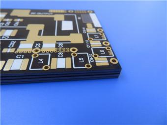
Wangling F4BTM300 Custom 2-layer PCB 20mil DK3.0 Substrate with Immersion Gold

RF-10 25mil Taconic PCB Materials stands out as a high-performance solution for RF applications. Its exceptional electrical properties, dimensional stability, thermal conductivity, and adhesion characteristics make it an ideal choice for demanding applications.
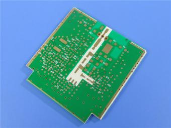
The PCB has a 4-layer hybrid stackup with a 0.5oz+plating ground layer, two 1oz ground layers, and a 0.5oz+plating signal layer.
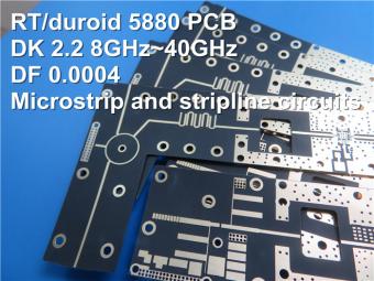
The dimensions of the board are 55.00 x 26.00 mm, with a tolerance of +/- 0.15mm. The board has 16 components, 26 total pads, 9 through-hole pads, 10 top SMT pads, 7 bottom SMT pads, 77 vias, and 82 nets.
Rogers RO4003C PCB is an innovative and advanced circuit board that is made with high-quality materials.
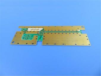
The RO4350B PCB offers a range of benefits that make it an ideal choice for high-frequency applications. Its low dielectric loss and high thermal conductivity make it perfect for high-frequency applications such as RF and microwave circuits.

Bicheng PCB Ships High-Quality PCBs with Shengyi Tg150 ℃ S1000H Material and Advanced Stackup
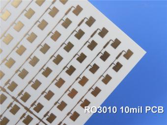
Rogers RO3010 PCB is ideal for a wide range of high-frequency applications, including power amplifiers, filters, couplers, and antennas.
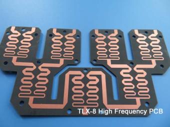
TLX-8 features low dielectric loss, low moisture absorption, and excellent thermal stability, making it ideal for high-frequency and high-speed applications. It has a low dissipation factor, which helps to minimize signal loss and distortion.
 6-11C Shidai Jingyuan, Fuyong, Baoan, Shenzhen, Guangdong, China 518103


For inquiries about our products or pricelist, please leave to us and we will be in touch within 24 hours.
© Copyright: 2026 Shenzhen Bicheng Electronics Technology Co., Ltd.. All Rights Reserved.

IPv6 network supported


