

 Call Us Now !
Tel : +86 755 27374946
Call Us Now !
Tel : +86 755 27374946
 Order Online Now !
Email : info@bichengpcb.com
Order Online Now !
Email : info@bichengpcb.com
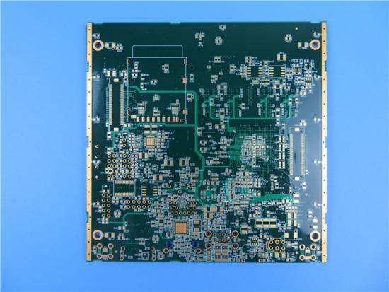
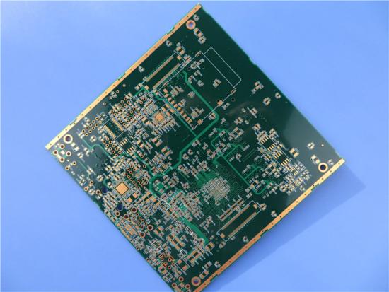
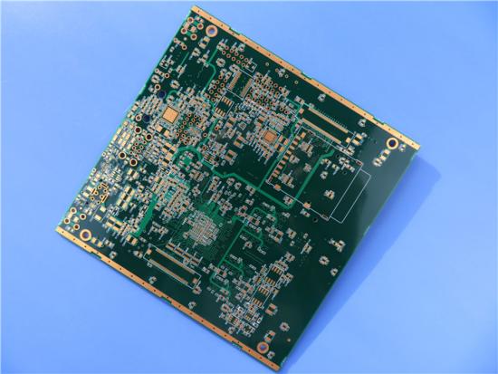
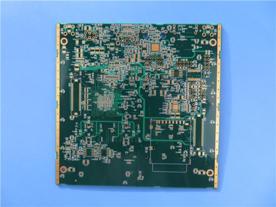
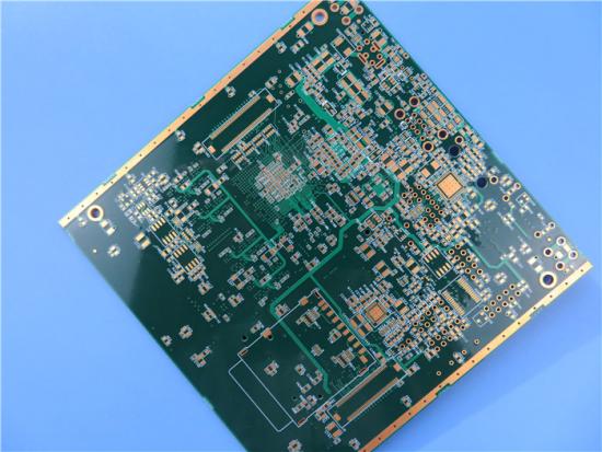
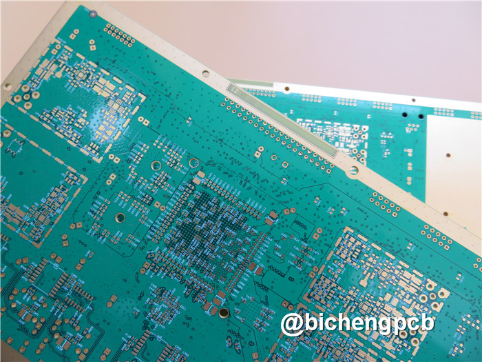
This is a type of 10-layer PCB circuit board
built on FR-4 substrate with Tg 180°C for the application of signal generator.
Item NO.:
BIC-474-v47.0Order(MOQ):
1-10Payment:
T/TProduct Origin:
ChinaShipping Port:
ShenzhenLead Time:
7-10 daysPrinted Circuit Board with 90 Ohm Impedance Controlled | Single End Impedance Differential Impedance PCB Board
(Printed Circuit Boards are custom-made products, the picture and parameters shown are just for reference)
1.1 General Description:
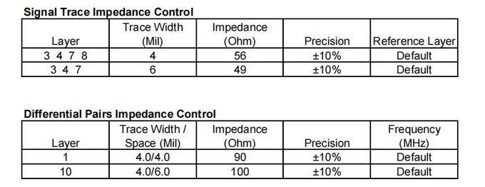
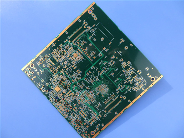
It's 1.6 mm thick with white silkscreen(Taiyo) on green solder mask (Taiyo) and immersion gold on pads. It's also an impedance controlled PCB with single-end impedance in inner layers and differential impedance controlled on top and bottom layer. The base material is from ITEQ. They're fabricated per IPC 6012 Class 2 using supplied Gerber data. Each 25 boards are packed for shipment.
1.2 Features and Our Advantages:
1) High Tg materials shows excellent thermal reliability and CAF resistance providing long-term reliability for industrial and automobile application.
2) Gold pads have good oxidation resistance and good heat dissipation.
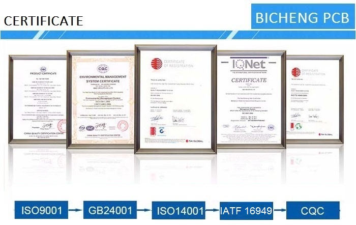
3) UL, ISO14001, IATF16949 certified factories
4) Higher than 98% on-time-delivery rate.
5) Customer complaint rate: <1%
6) No minimum order quantity. 1 piece is available
1.3 Applications:
Modems, Data Logger, Wireless N Router, Modem Router Wireless, 24V Transformer, 3G USB, PLC Program, Embedded Development, Master Module, Computers
1.4 PCB Data Sheet:
| PCB SIZE | 99.1 x 105.3mm=1PCS |
| BOARD TYPE | Multilayer PCB |
| Number of Layers | 10 Layers |
| Surface Mount Components | YES |
| Through Hole Components | YES |
| LAYER STACKUP | copper ------- 17.5um(0.5oz)+plate TOP Signal |
| 4mil prepreg 2113 | |
| copper ------- 35um(1oz) GND Plane | |
| 5mil FR-4 | |
| copper ------- 18um(0.5oz) SIG1 | |
| 5mil prepreg 2116 | |
| copper ------- 18um(0.5oz) SIG2 | |
| 5mil FR-4 | |
| copper ------- 35um(1 oz) PWR Plane | |
| 13mil prepreg 7628 + 1080 | |
| copper ------- 35um(1 oz) GND Plane | |
| 5mil FR-4 | |
| copper ------- 18um(0.5oz) SIG3 | |
| 5mil prepreg 2116 | |
| copper ------- 18um(0.5oz) SIG4 | |
| 5mil FR-4 | |
| copper ------- 35um(1oz) GND Plane | |
| 4mil prepreg 2113 | |
| copper ------- 17.5um(0.5oz)+plate BOT Signal | |
| TECHNOLOGY | |
| Minimum Trace and Space: | 4mil/4mil |
| Minimum / Maximum Holes: | 0.3/5.5mm |
| Number of Different Holes: | 31 |
| Number of Drill Holes: | 3532 |
| Number of Milled Slots: | 0 |
| Number of Internal Cutouts: | 0 |
| Impedance Control | Single-Ended Trace Width: L3 / L4 / L7 / L8 --- 4mils --- 56 ohm, L3 / L4 / L 7 --- 6mils --- 49 ohm; Differential impedance: L1 --- 4 mils / 4 mils --- 90 ohm; L10 --- 4 mils / 6 mils --- 100 ohm |
| BOARD MATERIAL | |
| Glass Epoxy: | FR-4, ITEQ IT-180 TG>170, er<5.4 |
| Final foil external: | 1oz |
| Final foil internal: | 0.5oz |
| Final height of PCB: | 1.6mm ±0.16 |
| PLATING AND COATING | |
| Surface Finish | Immersion Gold (12.8%) 2µ" over 100µ" nickel |
| Solder Mask Apply To: | Top and Bottom, 12micon Minimum. |
| Solder Mask Color: | Green, PSR-2000GT600D, Taiyo supplied |
| Solder Mask Type: | LPSM |
| CONTOUR/CUTTING | Routing |
| MARKING | |
| Side of Component Legend | TOP and Bottom. |
| Colour of Component Legend | White, IJR-4000 MW300, Taiyo Supplied. |
| Manufacturer Name or Logo: | Marked on the board in a conductor and leged FREE AREA |
| VIA | Plated Through Hole(PTH), Via in Pad and via tented and not be visible. |
| FLAMIBILITY RATING | UL 94-V0 Approval MIN. |
| DIMENSION TOLERANCE | |
| Outline dimension: | 0.0059" (0.15mm) |
| Board plating: | 0.0030" (0.076mm) |
| Drill tolerance: | 0.002" (0.05mm) |
| TEST | 100% Electrical Test prior shipment |
| TYPE OF ARTWORK TO BE SUPPLIED | email file, Gerber RS-274-X, PCBDOC etc |
| SERVICE AREA | Worldwide, Globally. |
1.5 Single ended (line) impedance, Differential impedance:
Definition of Characteristic Impedance
At a certain frequency, relative to a reference layer, the resistance of its high-frequency signals or electromagnetic waves in the process of transmission is called the characteristic impedance, which is the vector summation of electrical impedance, inductive reactance, capacitance resistance.
The classification of characteristic impedance
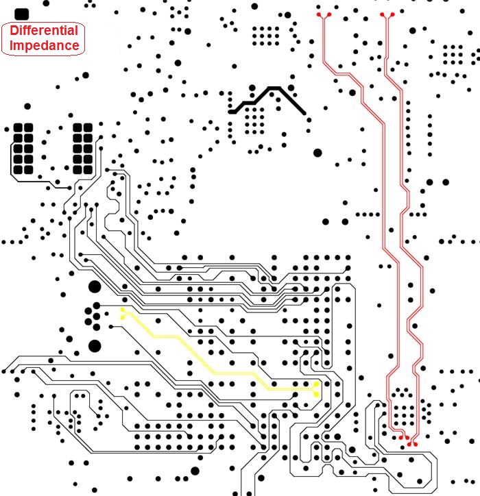
Common characteristic impedance is divided into:(1)Single ended (line) impedance; (2) Differential impedance and (3) coplanar impedance, etc.
Single ended impedancerefers to the measured impedance of a single signal line.Differential impedancerefers to the impedance measured between the two transmission lines with equivalent width and spacing in differential drive.Coplanar impedancerefers to the impedance measured when the signal line is transmitting between its surrounding GND / VCC (the space between the signal line to GND / VCC on both sides is equal).
The Determinant Condition Required for Impedance Control
When the signal is transmitted in the PCB conductor, if the length of conductor is close to the 1/7 of the signal wavelength, then the conductor at this time becomes a signal transmission line, the other general signal transmission lines are required to be done with impedance control. Whether it is required to control the impedance in PCB production is based on the customer's requirement, if the customer requires that a certain line width need to be done with impedance control, it is required to control the impedance of the line width in production.Three basic elements of impedance match are the output impedance (the original active parts), the characteristic impedance (signal line), the input impedance (passive parts) (PCB board)
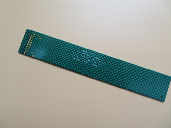
More Displays of Impedance Controlled PCB:
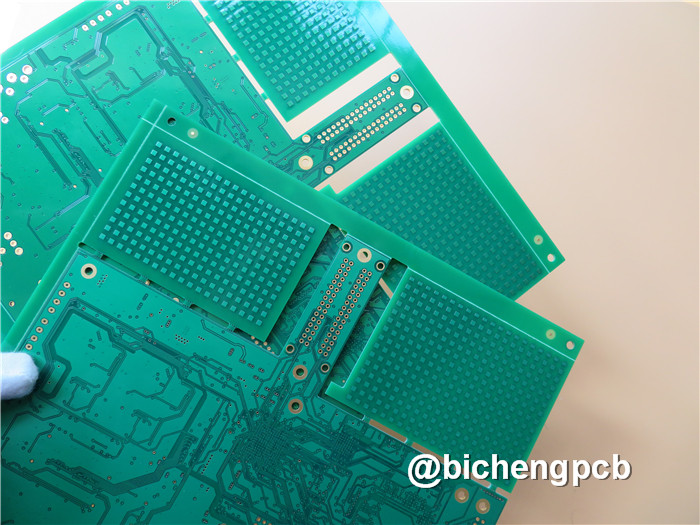
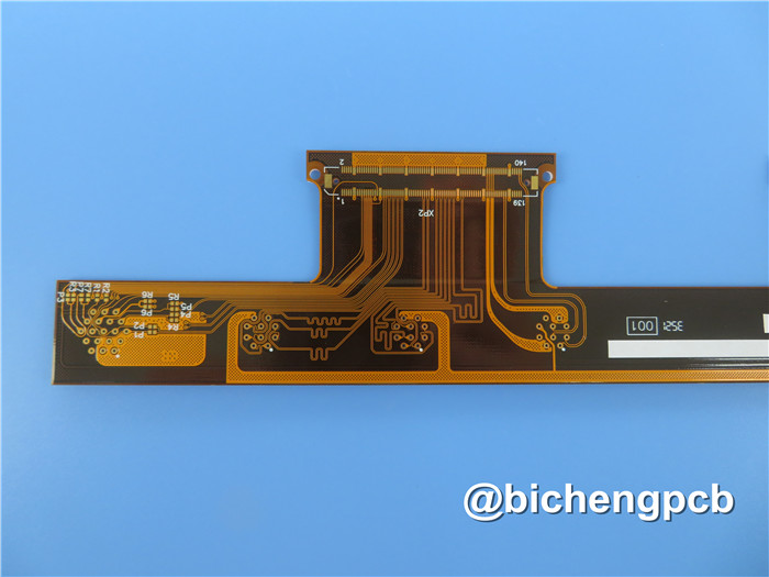
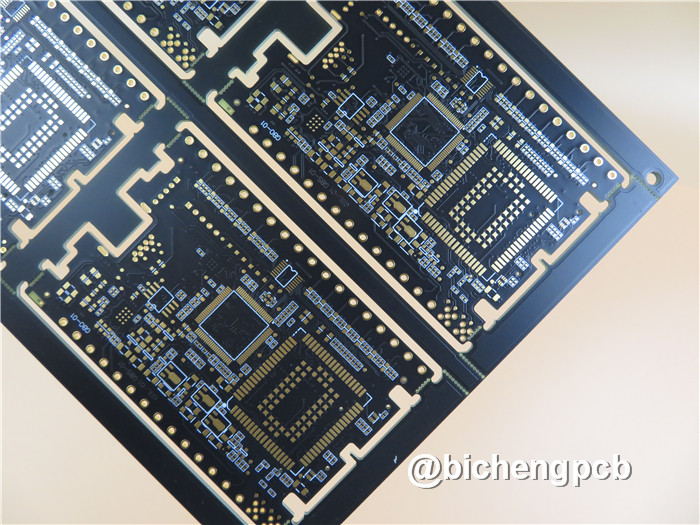
BICHENG MAIN COURIERS:

If you have questions or suggestions,please leave us a message,we will reply you as soon as we can!
Categories
New Products
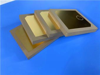
Wangling TP2200 PCB 0.8mm Substrate Immersion Gold 2-Layer High-Dk (Dk 22) RF Board
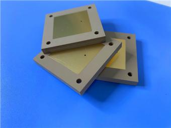
Rogers TMM10 PCB 5.08mm Core ENIG 2-Layer High-Dk Microwave Board
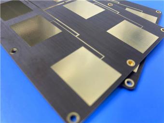
Taconic TLX-8 PCB 50mil ENIG 2-Layer High-Frequency RF Circuit Board
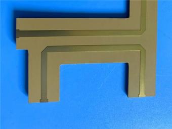
Wangling TF440 25mil DK4.4 Laminate Immersion Gold 2-Layer Copper-filling Vias PCB
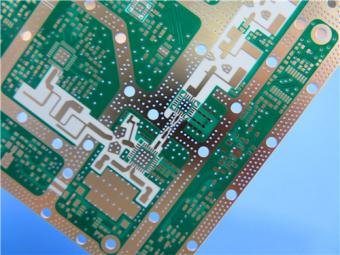
RO4360G2 Rogers 12mil ENEPIG 2-Layer DK6.15 High Frequency Custom PCB
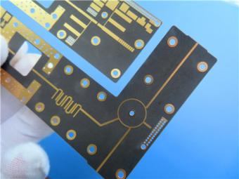
Wangling F4BTMS220 2-Layer DK2.2 PCB 10 mil Core with Immersion Gold
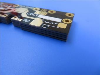
Wangling F4BTME350 10mil DK3.5 High Frequency Substrate PCB 2-Layer Immersion Gold
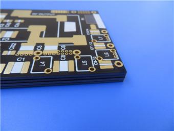
Wangling F4BTM300 Custom 2-layer PCB 20mil DK3.0 Substrate with Immersion Gold
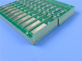
This is a type of high Tg PCB with differential impedance on layer 3 at 6mil/7mil, 6mil/10mil.
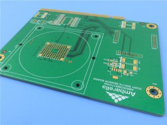
This is a type of low loss high performance multi-layer PCB built on TUC’s TU-883 core with 20 copper layers (20-layer PCB).
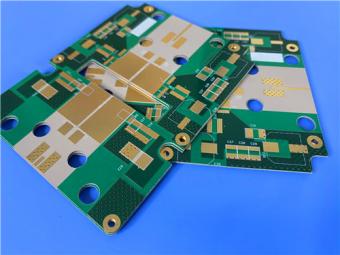
RO3203 10mil Rogers substrate PCB delivers the precision, stability, and value your project demands.
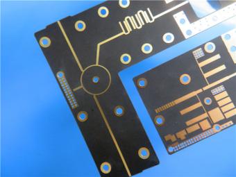
Rogers' TC350 is a woven fiberglass reinforced, ceramic filled, PTFE based composite for use as making printed circuit board.
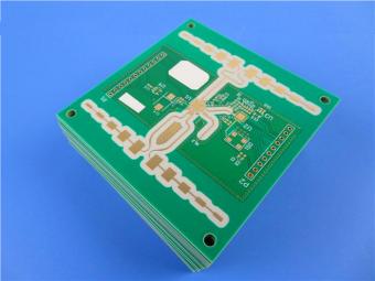
The Rogers CLTE-XT is a composite laminate that is filled with tiny-dispersed filler ceramics.
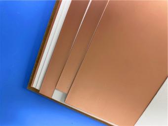
F4BME245 is a premium PTFE-based copper clad laminate manufactured by Taizhou Wangling Insulation Material Factory.
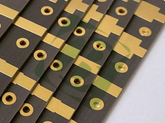
The TLY-3 Taconic High Frequency PCB is engineered to bridge the gap between high-frequency performance and manufacturing efficiency.
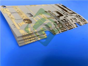
The RT/duroid 6035HTC 30mil substrate PCB is a high-performance solution for engineers needing to balance power, thermal management, and cost.
 6-11C Shidai Jingyuan, Fuyong, Baoan, Shenzhen, Guangdong, China 518103


For inquiries about our products or pricelist, please leave to us and we will be in touch within 24 hours.
© Copyright: 2026 Shenzhen Bicheng Electronics Technology Co., Ltd.. All Rights Reserved.

IPv6 network supported


