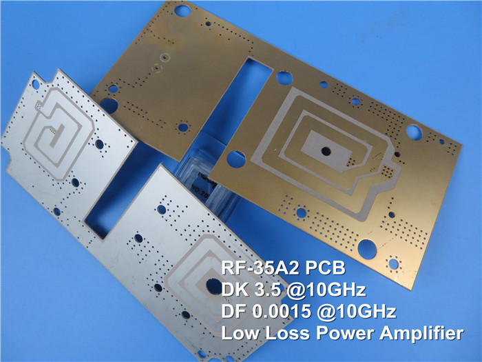
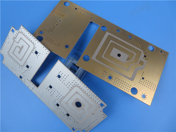
Introduction of RF-35A2
RF-35A2 laminate is a cutting-edge printed circuit board (PCB) designed specifically for high-frequency applications. Engineered with an ultra-low fiberglass content, RF-35A2 achieves "best in class" insertion loss properties and maintains a homogeneous dielectric constant throughout the laminate. This advanced composition ensures exceptional signal integrity and reliability, making RF-35A2 PCB the ideal choice for demanding RF and microwave circuits.
In addition to its outstanding electrical properties, RF-35A 25mil material exhibits a uniform dispersion of ceramic materials, resulting in extremely low coefficients of thermal expansion along the x and y axes. This unique feature, combined with its low modulus, makes RF-35A2 an excellent material for the surface mounting of chip carriers, further enhancing its versatility and applicability.
Manufactured using a proprietary multi-step process, RF-35A2 Substrate not only offers superior dielectric properties but also boasts excellent copper peel adhesion. With a dissipation factor as low as 0.0015 at 10 GHz, this PCB enables maximum power transfer and minimizes heat generation, ensuring optimal performance even under high-frequency and high-power conditions.

Features
Taconic RF-35A2 comes with an array of features that set it apart in the realm of high-frequency PCBs:
1.Ultra Low Loss Power Amplifier Substrate:
RF-35A2 is specifically designed to provide exceptional signal transmission with minimal loss, making it an ideal choice for high-performance power amplifiers.
2.Dielectric Constant (Dk) of 3.5 at 10 GHz:
The homogeneous dielectric constant of RF-35A2 ensures consistent electrical characteristics throughout the entire board, enabling precise signal propagation and minimizing signal distortion.
3.Dissipation Factor of 0.0015 at 10 GHz/23°C:
RF-35A2's ultra-low dissipation factor allows for efficient power transfer and reduces heat generation, ensuring stable and reliable performance.
4.X-CTE of 10 ppm/°C, Y-CTE of 13 ppm/°C, Z-CTE of 108 ppm/°C:
The low coefficients of thermal expansion in RF-35A2 provide excellent dimensional stability, minimizing the risk of delamination and ensuring consistent performance across a wide range of temperatures.
5.Peel Strength (1 oz. VLP) of 12 lbs/in:
RF-35A2 exhibits exceptional copper peel strength, ensuring reliable adhesion between the copper foil and the substrate, even in demanding environments.
6.Td of 528°C:
RF-35A2 is capable of withstanding high-temperature applications, ensuring its suitability for a wide range of industries and environments.
7.Moisture Absorption of 0.03%:
With its low moisture absorption rate, RF-35A2 offers excellent reliability and stability, even in high-humidity conditions.
Benefits
Using RF-35A2 as the foundation for your high-frequency circuits provides several key benefits:
1.Low Loss Properties:
RF-35A2's ultra-low loss characteristics enable precise signal transmission and ensure minimal signal degradation, resulting in improved overall system performance.
2.Dk Tolerance of ±0.05:
The homogeneous dielectric constant, coupled with a tight tolerance of ±0.05, guarantees consistent electrical properties throughout the PCB, allowing for accurate design and predictable performance.
3.Homogeneous Dk:
RF-35A2 maintains a uniform dielectric constant, eliminating variations that can lead to impedance mismatches and signal integrity issues.
4.Excellent Peel Strength:
The superior copper peel adhesion of RF-35A2 ensures the reliability and durability of the PCB, even in demanding applications and harsh environments.
5.Low Moisture Absorption:
RF-35A2's minimal moisture absorption rate ensures the stability and long-term performance of the PCB, making it ideal for applications subjected to humidity and moisture.
6.Ease of Drilling:
RF-35A2 is highly machinable, allowing for precise drilling and easy fabrication, facilitating the manufacturing process and reducing production time.
PCB Stackup: 2-layer rigid PCB
2-layer RF-35A2 is available as a rigid PCB with the following stackup:
Copper_layer_1: 35 μm
RF-35A2: 0.127 mm (5mil)
Copper_layer_2: 35 μm
This stackup provides a balanced design that ensures optimal signal integrity and efficient power distribution.
PCB Construction Details
RF-35A2 PCBs are manufactured to meet the highest quality standards and come with the following construction details:
Board Dimensions: The PCB dimensions are precisely controlled, with an accuracy of 76.04mm x 33.18mm (±0.15mm), ensuring compatibility with various electronic devices and applications.
Minimum Trace/Space: RF-35A2 supports a minimum trace width and spacing of 5/5 mils, allowing for intricate and compact designs while maintaining signal integrity.
Minimum Hole Size: The minimumhole size supported by RF-35A2 PCBs is 0.45mm, enabling the use of smaller components and ensuring efficient routing.
No Blind Vias: RF-35A2 PCBs do not include blind vias, simplifying the manufacturing process and reducing production costs.
Finished Board Thickness: The finished thickness of RF-35A2 PCBs is 0.25mm, providing a slim profile for space-constrained applications.
Finished Cu Weight: The outer layers of RF-35A2 PCBs feature a finished copper weight of 1 oz (1.4 mils), striking a balance between conductivity and weight.
Via Plating Thickness: RF-35A2 PCBs come with a via plating thickness of 20 μm, ensuring reliable signal interconnection and maximizing electrical performance.
Surface Finish: To enhance performance and protect the PCB, RF-35A2 PCBs are finished with immersion silver, which provides excellent solderability and corrosion resistance.
Top Silkscreen and Bottom Silkscreen: RF-35A2 PCBs do not include top or bottom silkscreen, allowing for a clean and minimalist appearance while maintaining functionality.
Top and Bottom Solder Mask: RF-35A2 PCBs do not feature top or bottom solder mask, offering flexibility for specific applications where solder mask is not required.
100% Electrical Test: Each RF-35A2 PCB undergoes a rigorous 100% electrical test prior to shipment, ensuring that every board meets the required specifications.
PCB Statistics
RF-35A 25mil PCBs exhibit the following statistics:
Components: RF-35A2 PCBs support up to 23 components, providing flexibility for various circuit designs.
Total Pads: There are a total of 56 pads available on RF-35A2 PCBs, allowing for efficient component placement and interconnection.
Thru-Hole Pads: RF-35A2 PCBs feature 45 thru-hole pads, enabling the use of traditional through-hole components.
Top SMT Pads: RF-35A2 PCBs accommodate 11 surface-mount technology (SMT) pads on the top layer, facilitating the integration of SMT components.
Bottom SMT Pads: RF-35A2 PCBs do not include bottom SMT pads, making them suitable for single-sided SMT assembly or mixed technology designs.
Vias: RF-35A2 PCBs incorporate 24 vias, providing essential interconnection between different layers and ensuring reliable signal transmission.
Nets: RF-35A2 PCBs support 2 nets, allowing for efficient routing and interconnection of signals.

Type of Artwork Supplied: Gerber RS-274-X
RF-35A2 PCBs utilize Gerber RS-274-X files for the artwork, ensuring compatibility with standard PCB design software and facilitating the manufacturing process.
Accepted Standard: IPC-Class-2
RF-35A2 PCBs adhere to the widely recognized IPC-Class-2 standard, ensuring high-quality manufacturing and reliable performance.
Availability: Worldwide
RF-35A 25mil substrate PCBs are available for purchase worldwide, making them accessible to customers and manufacturers across the globe.
Some Typical Applications
RF-35A2 PCBs find application in a wide range of industries and electronic devices, including:
1.Power Amplifiers:
RF-35A2's low-loss properties and high-frequency capabilities make it an excellent choice for power amplifier designs, enabling efficient and reliable amplification of signals.
2.Filters/Couplers:
With its exceptional signal integrity and precise electrical characteristics, RF-35A2 PCBs are ideal for the construction of filters and couplers, ensuring accurate frequency response and minimal insertion loss.
3.High-Speed Digital:
RF-35A2 supports high-speed digital circuits, allowing for the transmission of data at ultra-high frequencies with minimal signal degradation and reliable performance.
4.Passive Components:
RF-35A2 PCBs provide a reliable platform for passive components such as resistors, capacitors, and inductors, ensuring optimal electrical performance and stability.
5.Wireless Antennas:
RF-35A2's low-loss properties and excellent signal transmission capabilities make it an excellent substrate material for wireless antennas, enabling efficient and reliable wireless communication.
Conclusion
In conclusion, RF-35A2 high frequency PCBs revolutionize high-frequency electronics with their ultra-low loss properties, homogeneous dielectric constant, and exceptional thermal stability. With a wide range of features, benefits, and applications,Taconic RF-35A2 PCBs are the go-to choice for demanding RF and microwave circuits, power amplifiers, filters, high-speed digital designs, passive components, and wireless antennas. Embrace the future of high-frequency electronics with RF-35A2 PCB, where performance and reliability meet innovation.

 Call Us Now !
Tel : +86 755 27374946
 Order Online Now !
Email : info@bichengpcb.com


