

 Call Us Now !
Tel : +86 755 27374946
Call Us Now !
Tel : +86 755 27374946
 Order Online Now !
Email : info@bichengpcb.com
Order Online Now !
Email : info@bichengpcb.com
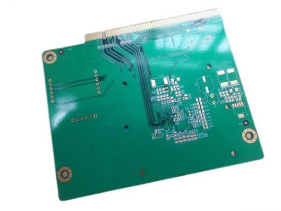
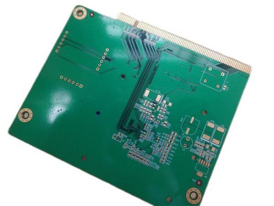
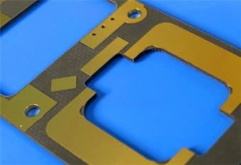
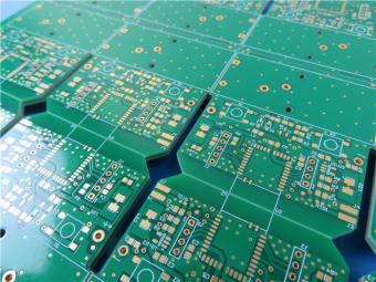
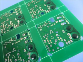
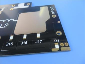
This is a type of 8-layer printed circuit board built on FR-4 substrate with Tg 170°C for the application of Mobile Broadband.
Item NO.:
BIC-459-v94.0Order(MOQ):
1-10Payment:
T/TProduct Origin:
ChinaShipping Port:
ShenzhenLead Time:
7-10 days
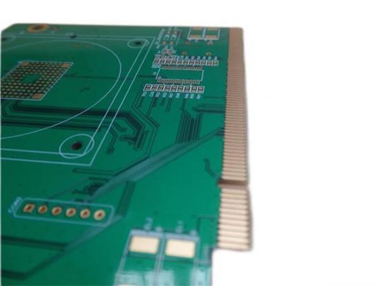
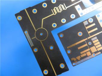
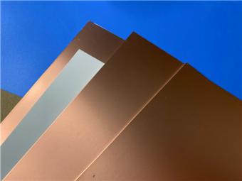
Gold Finger PCB Gold-plated Edge Connector Circuit Board Hard Gold Contact Fingers PCB
(Printed circuits boards are custom-made products, the picture and parameters shown are just for reference)
1.1 General description
It's 1.6 mm thick with white silkscreen(Taiyo) on green solder mask (Taiyo) and Immersion gold on pads. 80 strips of gold fingers are on edge for inserting usage.The base material is from Taiwan ITEQ supplying 1 up PCB per panel. They're fabricated per IPC 6012 Class 2 using supplied Gerber data. Each 25 boards are packed for shipment.
1.2 Features and benefits
1. High Tg material shows excellent thermal reliability and CAF resistance providing long-term reliability for industrial and automobile application;
2. Gold fingers reduce contact resistance;
3. 16000㎡workshop;
4. Meeting your PCB needs from prototype to mass production.
5. Strict WIP inspection and monitoring as well as working instruction;
6. IPC Class 2 / IPC Class 3;
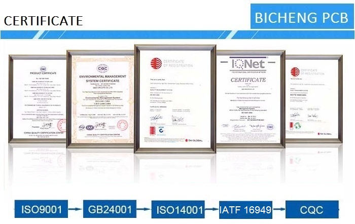
7. ISO9001, ISO14001, ISO13485, UL certified manufacturing factory;
8. Diversified shipping method: FedEx, DHL, TNT, EMS;
9. No MOQ, low cost for prototypes and small runs quantity.

1.3 PCB Specifications
| PCB SIZE | 150 x 141mm=1PCS |
| BOARD TYPE | Multilayer PCB |
| Number of Layers | 8 layers |
| Surface Mount Components | YES |
| Through Hole Components | NO |
| LAYER STACKUP | copper ------- 18um(0.5oz)+plate TOP layer |
| Prepreg 7628(43%) 0.195mm | |
| copper ------- 35um(1oz) MidLayer 1 | |
| FR-4 0.2mm | |
| copper ------- 35um(1oz) MidLayer 2 | |
| Prepreg 7628(43%) 0.195mm | |
| copper ------- 35um(1oz) MidLayer 3 | |
| FR-4 0.2mm | |
| copper ------- 35um(1oz) MidLayer 4 | |
| Prepreg 7628(43%) 0.195mm | |
| copper ------- 35um(1oz) MidLayer 5 | |
| FR-4 0.2mm | |
| copper ------- 35um(1oz) MidLayer 6 | |
| Prepreg 7628(43%) 0.195mm | |
| copper ------- 18um(0.5oz)+plate BOT Layer | |
| TECHNOLOGY | |
| Minimum Trace and Space: | 4mil/4mil |
| Minimum / Maximum Holes: | 0.35/3.5mm |
| Number of Different Holes: | 23 |
| Number of Drill Holes: | 183 |
| Number of Milled Slots: | 0 |
| Number of Internal Cutouts: | 0 |
| Impedance Control | no |
| Number of Gold finger | 39 |
| BOARD MATERIAL | |
| Glass Epoxy: | FR-4, ITEQ IT-180 TG170℃ er<5.4 |
| Final foil external: | 1oz |
| Final foil internal: | 1oz |
| Final height of PCB: | 1.6mm ±0.16 |
| PLATING AND COATING | |
| Surface Finish | Immersion gold on pad, electroplated gold on edge connectors |
| Solder Mask Apply To: | TOP and Bottom, 12micron Minimum |
| Solder Mask Color: | Gloss Green, Taiyo PSR-2000GT600D |
| Solder Mask Type: | LPSM |
| CONTOUR/CUTTING | Routing |
| MARKING | |
| Side of Component Legend | TOP and Bottom. |
| Colour of Component Legend | White, Taiyo IJR-4000 MW300 |
| Manufacturer Name or Logo: | Marked on the board in a conductor and leged FREE AREA |
| VIA | Plated through hole(PTH) |
| FLAMIBILITY RATING | UL 94-V0 Approval MIN. |
| DIMENSION TOLERANCE | |
| Outline dimension: | 0.0059" |
| Board plating: | 0.0029" |
| Drill tolerance: | 0.002" |
| TEST | 100% Electrical Test prior shipment |
| TYPE OF ARTWORK TO BE SUPPLIED | email file, Gerber RS-274-X, PCBDOC etc |
| SERVICE AREA | Worldwide, Globally. |
1.4 Applications
Bluetooth Transmitter
HDMI Splitters
CCTV Systems
Led Street Lights
Low Noise Amplifier
Door Access Control System
5G Mobile Hotspot
Multicoupler
Embedded Systems Development
Smart Phone and Cell Phone

1.5 Gold finger PCB
The Purpose is to establish electrical connection to the board without using a two-part connector system. Plating of nickel and gold is carried out in essentially the same way as plating copper and tin/lead, i.e., by electrolytic deposition. Plating can be carried out either manually or automatically. In the manual process, boards are more or less stationary in the gold plating bath, which causes a varying gold deposition along the row of contact fingers. The result will frequently be a thickness distribution with the outermost contact fingers having perhaps twice as much deposited gold as the center contact fingers. In the automatic process, gold plating takes place while the boards slide through the plating cell. The method offers a gold thickness variation that can be controlled within±5% or better. This is because all contact fingers will be dealt with in exactly the same way when the board moves through the process cell.
Edge connectors are frequently provided with a slot that serves to guide the board with respect to the receptacle (locating slot) and/or to prevent incorrect insertion of the board (polarization slot). Usually, the PCB manufacturer prefers to route the slot simultaneously with the contouring of the board. Obviously, this requires that the slot be slightly wider than the router bit used.
In order to ease the insertion of the board into the receptacle, the edge along the connector should be bevelled. The bevelling also has the advantage of reducing the scraping of the contacts of the receptacle when the board is inserted in the receptacle.

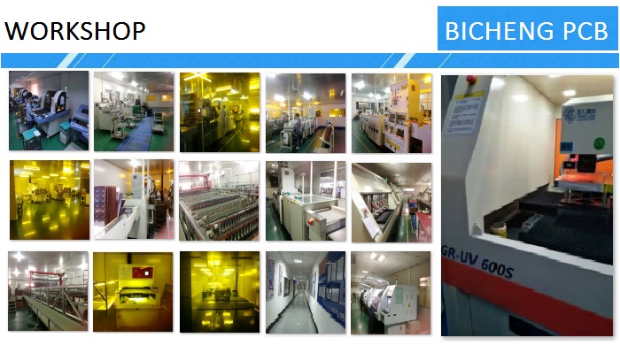
BICHENG PCB WORKSHOP:
BICHENG MAIN COURIERS:

Previous:
PCB with Ball Grid Array 10-Layer BGA Built On High Tg FR-4 With Immersion GoldNext:
PCB with Peelable Mask Double Sided Circuit Board Built on Tg170 FR-4 Coating HASL.If you have questions or suggestions,please leave us a message,we will reply you as soon as we can!
Categories
New Products
30mil Taconic CER-10 2-layer Immersion Silver DK10 High Frequency Laminate PCB
31mil Rogers RT/duroid 5880 Double-sided Bare Copper ENIG Finished PCB
Wangling TFA294 Laminate 40mil Immersion Silver No Solder Mask Silkscreen Custom PCB
50mil TMM6 PCB 2-layer EPIG Rogers DK6.0 Substrate No Solder Mask Silkscreen
60mil TMM10 PCB 1-layer OSP Microwave High Frequency Laminate No Solder Mask
Wangling F4BTMS265 Custom PCB 30mil 2-layer ENIG Black Solder Mask White Silkscreen
RO4835 20mil Rogers Laminate 2-layer Immersion Gold Custom PCB
Rogers 20mil DiClad 527 PCB 2-layer Immersion Gold No Solder Mask Black Silkscreen
Rogers Kappa 438 laminates were designed using a glass reinforced hydrocarbon ceramic system that offers superior high frequency performance and low cost circuit fabrication resulting in a low loss material which can be fabricated using standard epoxy/glass (FR-4) processes.
This is a type of low DK/DF FR-4 PCB which is built on TU-872 SLK Sp material.
This is a type of 2 layers PCB board built on FR-4 Tg170 substrate for the application of 8 Port Switch.
This is a type of 10-layer printed circuit board built on FR-4 Tg170 substrate for the application of PLC controls.
It’s 120mm long by 60mm wide with immersion gold on pads. Bottom layer is open to air with gold surface as we’ve seen.
RT/duroid 5880LZ PTFE-filled composite materials are engineered for demanding stripline and microstrip circuit applications.
The dielectric constant is stable and DK can be optional within the range of 3 to 22 according to the design of circuit requirement. The operating temperature is -100℃~+150℃.

Rogers RO3003 PCB is an excellent choice for high-frequency applications that require low loss, high thermal conductivity, and excellent electrical properties.
 6-11C Shidai Jingyuan, Fuyong, Baoan, Shenzhen, Guangdong, China 518103


For inquiries about our products or pricelist, please leave to us and we will be in touch within 24 hours.
© Copyright: 2026 Shenzhen Bicheng Electronics Technology Co., Ltd.. All Rights Reserved.

IPv6 network supported


