

 Call Us Now !
Tel : +86 755 27374946
Call Us Now !
Tel : +86 755 27374946
 Order Online Now !
Email : info@bichengpcb.com
Order Online Now !
Email : info@bichengpcb.com
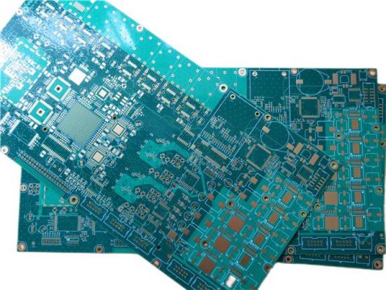
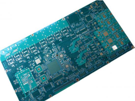
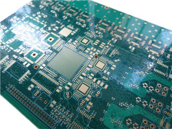
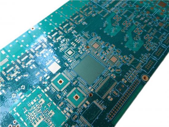
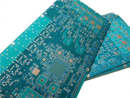
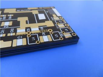
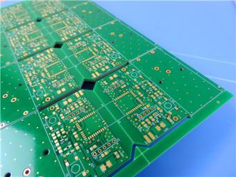
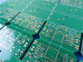
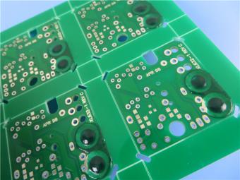
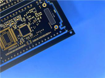
This is a type of 10-layer printed circuit board
built on FR-4 Tg170 substrate for the application of PLC controls.
Item NO.:
BIC-462-v97.0Order(MOQ):
1-10Payment:
T/TProduct Origin:
ChinaShipping Port:
ShenzhenLead Time:
7-10 days
PCB with Ball Grid Array 10-Layer BGA PCB Built On High Tg FR-4 With Immersion Gold
(Printed circuits boards are custom-made products, the picture and parameters shown are just for reference)
1.1 General description
It's 2.0 mm thick with white silkscreen on green solder mask and immersion gold on pads. A BGA package is placed on the top of the circuit board, high pin-count on a 0.5mm pitch. The base material is from Shengyi and supplying 1 up board. They're fabricated per IPC 6012 Class 2 using supplied Gerber data. Each 20 boards are packed for shipment.
1.2 Features and benefits
1. High Tg industrial standard material shows excellent thermal reliability;
2. Immersion gold ensure excellent wetting during component soldering and avoid copper corrosion;
3. In house, engineering design prevents problems from occurring in pre-production;
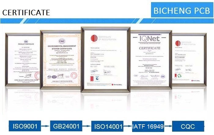
4. ISO9001, ISO14001, IATF16949, ISO13485, UL Certified;
5. Customer complaint rate: <1%
6. Delivery on time: >98%
7. Prototype PCB capability to Volume Production capability;
8. Multilayer and Any Layer HDI PCBs;
9. More than 18+ years of PCB experience.

1.3 Applications
Converter
USB Wireless Adapter
12V Inverter
Wireless Router Reviews
Ladder Logic
Battery Inverter
CCTV Security
Wireless G Router
Programmable Controllers
Backplanes
1.4 PCB Specifications
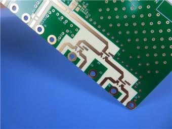
1.5 BGA and via plug
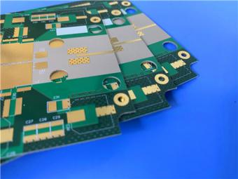
The full name of the BGA is Ball Grid Array, which is a type of surface mount package used for integrated circuit (IC). It has the characteristics of: ① packaging area reduced ② function increased and the number of pins increased ③ solder can be self-centered when dissolved soldering, easy to put on tin ④ reliability is high ⑤ electric performance is good and low cost etc. PCB board with BGA generally have more small holes. Mostly, via holes under BGA are designed to be 8~12mil in diameter by customers. Vias under BGA have to be plugged by resin, soldering ink is not allowed to be onto pads and no drilling on BGA pads. The plugged vias are 0.25mm, 0.3mm, 0.35mm, 0.4mm, 0.45mm, 0.5mm and 0.55mm.
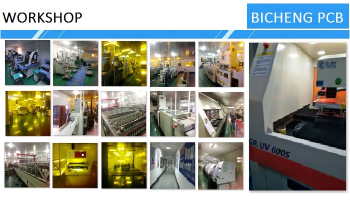
BICHENG PCB WORKSHOP:
BICHENG MAIN COURIERS:

Previous:
RF-35 High Tg High Frequency 30mil Double Sided PCB Immersion Gold and Black Solder MaskNext:
Gold Finger Gold-plated Edge Connector Circuit Board Hard Gold Contact Fingers PCBIf you have questions or suggestions,please leave us a message,we will reply you as soon as we can!
Categories
New Products
Wangling 5mil 0.127mm TFA300 Core 2-layer Immersion Gold Green Solder Mask PCB
7.5mil AGC Taconic TLY-5 Substrate Custom PCB EPIG Finish Bare Copper
10mil Rogers CuClad 250 Immersion Gold 2-Layer Rigid Microwave PCB
20mil F4BTMS450 Wangling DK4.5 Laminate Custom PCB HASL LF Finsh
F4BME275 Wangling DK2.75 Laminate 2-Layer 1.6mm Pure Gold RF Custom PCB
Wangling F4BTD350S High Frequency PCB 2-layer 20mil Thick ENIG DK3.5 Substrate
12-layer TG200 TU-872 SLK High-Speed FR4 1.68mm PCB with ENIG Impedance Control
12-Layer RO4350B + RO3010 3.14mm Hybrid PCB Nickel-Free EPIG Surface Finish Blind Via
Rogers Kappa 438 laminates were designed using a glass reinforced hydrocarbon ceramic system that offers superior high frequency performance and low cost circuit fabrication resulting in a low loss material which can be fabricated using standard epoxy/glass (FR-4) processes.
This is a type of low DK/DF FR-4 PCB which is built on TU-872 SLK Sp material.
This is a type of 2 layers PCB board built on FR-4 Tg170 substrate for the application of 8 Port Switch.
This is a type of 8-layer printed circuit board built on FR-4 substrate with Tg 170°C for the application of Mobile Broadband.
It’s 120mm long by 60mm wide with immersion gold on pads. Bottom layer is open to air with gold surface as we’ve seen.
It’s for the application of broadband wireless solutions. It's 2.0 mm thick, pads are immersion gold plated.
Our M6 High-Speed Low-Loss 6-Layer PCB is engineered for high-frequency, high-speed, and high-reliability applications, making it an ideal choice for 5G, automotive radar, data centers, and aerospace systems.
This 32mil TRF-45 Immersion Gold PCB integrates Taconic's industry-leading high-frequency laminate technology with precision PCB manufacturing to deliver a reliable, high-performance solution for demanding RF and microwave applications.
 6-11C Shidai Jingyuan, Fuyong, Baoan, Shenzhen, Guangdong, China 518103


For inquiries about our products or pricelist, please leave to us and we will be in touch within 24 hours.
© Copyright: 2026 Shenzhen Bicheng Electronics Technology Co., Ltd.. All Rights Reserved.

IPv6 network supported


