
 Call Us Now !
Tel : +86 755 27374946
Call Us Now !
Tel : +86 755 27374946
 Order Online Now !
Email : info@bichengpcb.com
Order Online Now !
Email : info@bichengpcb.com
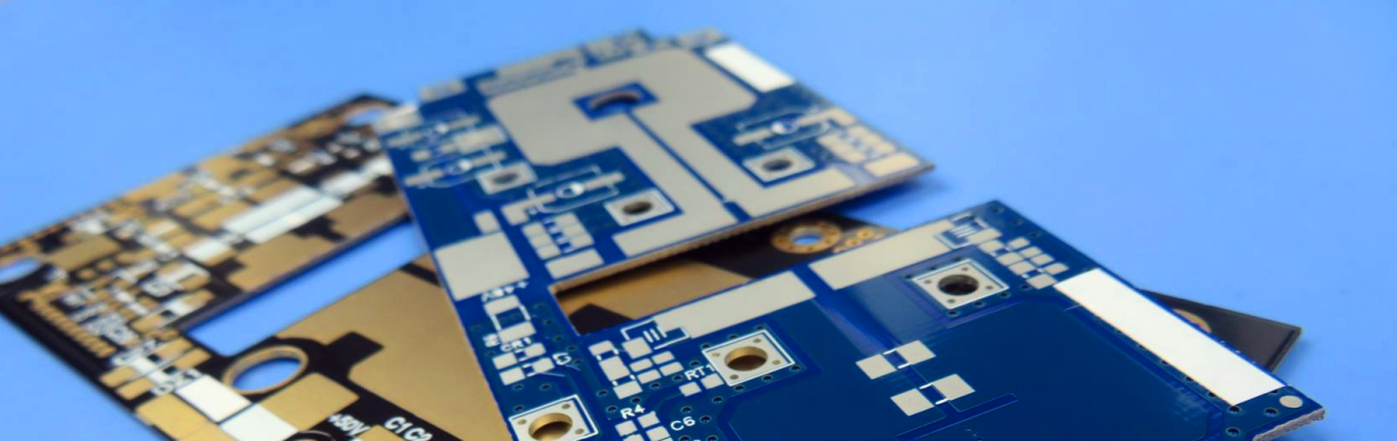
Aluminum Circuit Board Manufacturing and What Manufacturing Difficulties & Matters Needing Attention As the substrate material of PCB aluminum substrate manufacturing, aluminum clad plate mainly plays the role of interconnecting conduction, insulation and support to aluminum PCB substrate, and has great influence on signal transmission speed, energy loss and characteristic impedance in circuit. The performance, quality, manufacturability, manufacturing level, manufacturing cost, and long-term reliability and stability of PCB aluminum substrate are largely determined by aluminum clad copper plate. Aluminum based circuit boards have excellent electrical performance, heat dissipation, electromagnetic shielding, high dielectric strength and bending resistance. As a metal core PCB, whether it is single, double-side aluminum pcb or multi-layer aluminum circuit board, they have many similarities with FR4 circuit board in the manufacturing process, such as etching thick copper foil, aluminum surface etching protection, aluminum plate manufacturing and solder blocking printing. However, as a kind of advanced PCB, aluminum base PCB still has special aspects of manufacturing process, which requires strict and effective management and control. So, what are the precautions and manufacturing difficulties in aluminum based circuit board production? Machining: Drilling aluminum substrate can be done, but the inner edge of the drilled hole should not have any burrs, which will affect the pressure test. Milling the profile is very difficult. And the shape, the need to use advanced mold, mold production is very skilled, as one of the difficulties of aluminum substrate. After the shape is flushed, the edge is required to be very neat, without any burr, and does not touch the welding resistance layer of the plate edge. Usually use the soldier die, hole from the line, shape from the aluminum surface, circuit board when the force is on the shear pull, and so on are skills. After punching the shape, the warpage of the board should be less than 0.5%. The whole production process is not allowed to wipe the aluminum base surface: the aluminum base surface by hand touch, or by some chemicals will produce surface discoloration and blackening, which is absolutely unacceptable. Some customers do not accept the re-polishing of the aluminum base surface, so the whole process does not touch the aluminum base surface is one of the difficulties in the production of aluminum base circuit board. Some enterprises use passivation process, some in hot air leveling (tin spraying) before and after each affixed with a protective film many small skills, the eight imfairy across the sea, each brilliant. Over high voltage test: aluminum base plate of communication power supply requires 100% high voltage test. Some customers require DIRECT current, and some require alternating current. The voltage is 1500V and 1600V, and the time is 5 seconds and 10 seconds. Dirt, holes, aluminum edge...
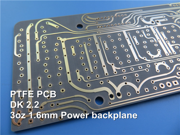
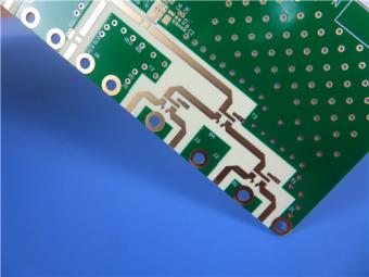
Why Do High Frequency PCB Boards Require Low Dielectric Constant? Why require high frequency PCB board low ε(Dk)? ε or Dk, called dielectric constant, is the ratio of the capacitance between the electrodes of a PCB filled with a certain substance and the capacitance of a vacuum capacitor of the same structure, usually indicates the size of a material to store electric energy. When the ε is large, the storage capacity is large, and the transmission speed of electrical signals in the circuit will become low. The current direction through the electrical signal on the PCB board is usually positive and negative alternating change, equivalent to the substrate for continuous charging, discharging process, in exchange, capacitance will affect the transmission speed, and this effect, in the high-speed transmission of the device is more important. Low ε means that the storage capacity is small, charging and discharging process is fast, so that the transmission speed is also fast. Therefore, in the transmission of high frequency PCB board, low dielectric constant is required. Another concept is dielectric loss. Dielectric materials under the action of alternating electric field, due to heat and energy consumption is called dielectric loss, usually expressed by dielectric loss factor Tan δ. ε and tanδ is proportional, high-frequency circuit also requires low ε, medium loss Tan δ is small, so the energy loss is small. Dielectric constant of high frequency PCB board Epsilon of Teflon printed board In the circuit board substrate, polytetrafluoron substrate dielectric constant ε is the lowest, typical only 2.6~2.7, and the general glass cloth epoxy resin substrate DIELECTRIC constant of FR4 is 4.6~5.0, therefore, Teflon circuit board signal transmission speed is much faster than FR4 (about 40%). Teflon boards have an intermediate loss factor of 0.002, 10 times lower than FR4's 0.02, and much lower energy loss. Plus polytetrafluoron known as "plastic king", excellent electrical insulation performance, chemical stability and thermal stability (so far there is not a solvent can dissolve it below 300℃), so high frequency high-speed signal transmission will first use Teflon or other low dielectric constant of the base material. Polyflon, Rogers, Taconic, Arlon, Meclad all provide substrates with dielectric constants of 2.10, 2.15, 2.17, 2.20, with a dielectric loss factor of 0.0005~0.0009 at 10GHZ. PTFE substrate performance is very good, but its processing into circuit board process with the traditional FR4 has a completely different process. These years, in addition to the requirements of ε 2.15, 2.6, but also often used ε3.38, 3.0, 3.2, 3.8 Rogers RO4000, GIL1000 series, etc. Basic requirements for HF PCB boards 1. Due to high frequency signal transmission, the characteristic impedance of the finished printed board wire is strictly required, and the wire width of the board is usually ±0.02mm(the strictest is ±0.015mm). Therefore, the etching process should be stri...
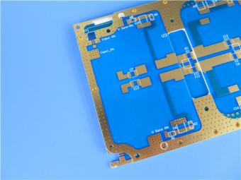
Let's Get to Know the High Frequency Substrate of 5G Era. With the development of electronic technology. The production of electronic products requires more and more materials, such as high-frequency materials. ROGERS PCB, for example, is a type of high-frequency board produced by ROGERS Company. Unlike conventional PCB board epoxies, it has no glass fiber in the middle and is a ceramic based high-frequency material. When the circuit operates at frequencies above 500MHz, the range of materials available to the design engineer is greatly reduced. Rogers RO4350B materials allow RF engineers to easily design circuits, such as network matching, impedance control of transmission lines, etc. Due to its low dielectric loss, R04350B has an advantage over ordinary circuit materials in high frequency applications. Its dielectric constant fluctuation with temperature is almost the lowest among similar materials. In a wide frequency range, its dielectric constant is quite stable 3.48, and the design recommended value 3.66. LoPra copper foil reduces insertion loss. This makes the material suitable for broadband applications. Rogers PCB materials ceramic HF substrate series classification: Rogers RO3000 series: PTFE circuit materials based on ceramic filling, Rogers models are: RO3003, RO3006, RO3010, RO3035 high frequency laminate. Rogers RT6000 series: Based on ceramic filled PTFE circuit material, designed for electronic and microwave circuits requiring high dielectric constant, Rogers models are: RT6006 dielectric constant 6.15, Duroid 6010 dielectric constant 10.2. Rogers TMM series: based on ceramic, hydrocarbon, thermosetting polymer composite materials, Rogers models: TMM3, TMM4, TMM6, TMM10, TMM10i, TMM13i. , etc. At present, the global 5G layout is accelerating. The traditional 3G/4G base station distributed architecture can be mainly divided into BBU, RRU and antenna feed system, among which RRU and antenna feed system are connected through feeders. Due to the increased risk of transmission loss under high frequency, the architecture of integrated RRU and antenna feed system can reduce signal loss on feeders and improve transmission efficiency. Highly integrated, a large number of scattered parts are replaced by PCB boards, which ultimately increases the unit usage of PCB. High frequency PCB material In the 5G era, high frequency bands must be used (3GPP has specified that 5GNR supports a frequency range of 450MHz to 52.6ghz) for the following reasons: 1) After the iteration of the first 4 generations of communication technology, the resources of low frequency band have been occupied, and the resources that can be used for 5G development are few; 2) The higher the frequency is, the more information can be loaded, the more resources are richer, and thus the transmission rate can be higher (for example, in 100MHz, only 5 channels of 20MHz can be divided, while 1GHz can be divided into 50 channels of 20MHz). Resonance phenomenon caused by the load and ...

Technical Requirements for 5G Millimeter Wave HF PCB Copper-clad Board As the development of electronic communication products has experienced several stages, such as 1G, 2G, 3G and 4G, and is now entering the stage of the 5th generation of communication products. As the 5th generation of electronic communication, compared with 4G, 5G has undergone great changes in peak rate, spectral efficiency, delay and other aspects, which puts forward new requirements for high frequency board and copper-clad plate materials. 5G communication to PCB technology requirements With the trend of miniaturization and increasing capacity of communication products, the design space of the front end of the product is severely squeezed. In order to relieve the design pressure, communication chip manufacturers have to choose to develop higher rate IC products to meet the demand of large capacity and small volume products. However, with the increase of speed, the pressure on signal integrity engineers is not alleviated but increased. High-speed products can be achieved by using less wiring, but the increase of speed directly leads to strict requirements on signal quality and less and less margin. Under 10Gbps signal, the UI of the signal can reach the bit width of 100ps, but under 25Gbps signal, the bit width of the signal is only 40ps, which means that optimization design should be carried out in every link of the channel to strive for the margin of every PS. 5G communication, as the fifth generation of mobile communication products, has applied many new technologies, but in any case, it cannot do without PCB as the carrier. The requirements for PCB are more and more stringent, especially for PCB substrate materials, processing technology, surface treatment and other very high requirements. The increasing working frequency of 5G communication products has brought new requirements to the manufacturing process of printed boards. Millimeter-wave PCBS are usually multi-layer structures, and microstrip lines and grounded coplanar waveguide circuits are usually located in the outermost layer of the multi-layer structure. Millimeter wave belongs to the very high frequency (EHF) range in the whole microwave field. The higher the frequency is, the higher the dimensional accuracy of the circuit is required. Comparison between 5G and 4G on PCB process capacity requirements 1. Appearance control requirements: The microstrip lines in key areas are not allowed to have pits and scratches, because the pcb stripline of high-frequency PCB transmit high-frequency electrical pulse signals instead of current. Pits, gaps, pinholes and other defects on high-frequency lines will affect transmission, and any such small defects are not allowed. 2. Control the corner of the microstrip antenna to improve the gain, direction and standing wave of the antenna; To avoid the resonance frequency deviation to high frequency and improve the margin of antenna design, it is necessary to control the Corner sh...
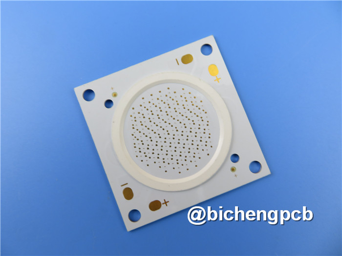
Have a knowledge of the difference between copper substrate and FR-4 Copper is one of the most expensive metal substrates and conducts heat many times better than aluminum and iron substrates. Aluminum substrate is generally a single layer, is a type of PCB board. Aluminum substrate is considered to be a generic term for PCB boards used specifically in the LED industry because of their good thermal conductivity. It is suitable for high frequency circuit heat dissipation, building decoration industry, high and low temperature change area, precision communication equipment, etc. LED aluminum substrate is divided into front and back. The white side is welded with LED pins and the other side is welded with aluminum. After coated with heat-conducting paste, it is used to contact heat-conducting parts. The high-end practical design is also a double panel which is divided into circuit layer, insulation layer, aluminum, insulation layer and circuit layer structure. Rarely used in multilayer board, ordinary multilayer board can be bonded with insulation layer and aluminum alloy. Aluminum substrate good heat dissipation, good processability, dimensional stability and electrical performance make it widely used in integrated circuits, automobiles, office suite software comparison, high-power electrical equipment, power equipment and other fields. Copper substrate is also divided into single panel, double panel and multi-layer plate according to the different number of layers. Compared with aluminum plate, copper plate due to special material, heat dissipation is relatively good, the price is relatively high. Widely used in high frequency circuit, high and low temperature change, precision communication equipment heat dissipation, building decoration and other industries. There are generally gold-impregnated copper substrate, silver-plated copper substrate, tin-sprayed copper substrate, copper oxide substrate and so on. The circuit layer of copper substrate requires a large current-carrying capacity, so thicker copper foil should be selected, the thickness is generally 35μm~280μm; The thermal conductive insulating layer is the core technology of copper substrate. The core thermal conductive composition is composed of aluminum oxide and silicon powder and epoxy resin filled polymer. It has low thermal resistance (0.15), excellent viscoelasticity, thermal aging resistance, and the ability to withstand mechanical and thermal stress. The metal base of copper substrate is the supporting member of copper substrate, which needs high thermal conductivity. Generally copper plate, suitable for drilling, punching and cutting and other conventional mechanical processing. The metal layer (block) mainly plays the role of heat dissipation, shielding, covering or grounding. Due to the difference of the performance of copper and aluminum and the corresponding PCB processing technology, copper substrate has more performance advantages than aluminum substrate. Hf board is gener...

Why High TG Materials Are Used in PCB Production? In addition to the basic FR-4 material in PCB production, some customers also indicate that high TG material should be used in the materials. Then why do they use high TG material in PCB production? Used in PCB production is the full name of the TG glass transition temperature, on behalf of the glass transition temperature. The circuit board must be flame resistant and cannot burn at a certain temperature, only to soften. This temperature point is called glass state transition temperature (Tg point), this value is related to the size stability of the PCB board. When the temperature rises to a certain area of TgPCB, the substrate will change from "glass state" to "rubber state", which is called the glass transition temperature of the sheet (TG). In other words, Tg is the substrate temperature that remains high (℃). That is to say, ordinary PCB substrate materials at high temperature, not only produce deformation, melting and other phenomena, but also on the mechanical and electrical properties of the sharp decline. Why high TG materials are used in PCB production? The increase of Tg base, the characteristics of heat resistance, moisture resistance, chemical resistance and resistance stability of Shenzhen circuit board proofing will be strengthened and improved. The higher the TG value, the better the temperature and other properties of the plate, especially in the lead-free manufacturing process, high TG is more widely used. High Tg refers to high heat resistance. With the rapid development of the electronic industry, especially the electronic products represented by computers are developing towards high functionalization and high multilayer, which requires the higher heat resistance of PCB substrate materials as an important guarantee. The appearance and development of high density installation technology represented by SMT and CMT make PCB more and more dependent on the support of high heat resistance of substrate in small aperture, fine line and thin form. This is also a big reason to use high TG materials in PCB production. Therefore, in PCB production, the difference between general FR-4 and high Tg FR-4 is that in the hot state, especially after hygroscopic heating, the material has differences in mechanical strength, dimensional stability, adhesion, water absorption, thermal decomposition, thermal expansion and other conditions, and the high Tg product is obviously better than the common PCB substrate material.
Categories
New Products
Wangling 5mil 0.127mm TFA300 Core 2-layer Immersion Gold Green Solder Mask PCB
7.5mil AGC Taconic TLY-5 Substrate Custom PCB EPIG Finish Bare Copper
10mil Rogers CuClad 250 Immersion Gold 2-Layer Rigid Microwave PCB
20mil F4BTMS450 Wangling DK4.5 Laminate Custom PCB HASL LF Finsh
F4BME275 Wangling DK2.75 Laminate 2-Layer 1.6mm Pure Gold RF Custom PCB
Wangling F4BTD350S High Frequency PCB 2-layer 20mil Thick ENIG DK3.5 Substrate
12-layer TG200 TU-872 SLK High-Speed FR4 1.68mm PCB with ENIG Impedance Control
12-Layer RO4350B + RO3010 3.14mm Hybrid PCB Nickel-Free EPIG Surface Finish Blind Via
 6-11C Shidai Jingyuan, Fuyong, Baoan, Shenzhen, Guangdong, China 518103


For inquiries about our products or pricelist, please leave to us and we will be in touch within 24 hours.
© Copyright: 2026 Shenzhen Bicheng Electronics Technology Co., Ltd.. All Rights Reserved.

IPv6 network supported


