

 Call Us Now !
Tel : +86 755 27374946
Call Us Now !
Tel : +86 755 27374946
 Order Online Now !
Email : info@bichengpcb.com
Order Online Now !
Email : info@bichengpcb.com
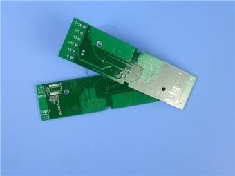
This is a type of 6 layer ultrathin printed
circuit board built on FR-4 substrate with Tg 135°C for the application of GPS
Tracking.
Item NO.:
BIC-460-v95.0Order(MOQ):
1-10Payment:
T/TProduct Origin:
ChinaShipping Port:
ShenzhenLead Time:
7-10 days
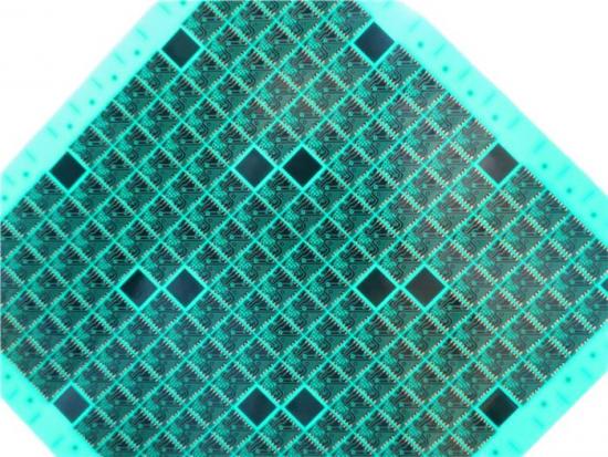
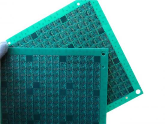
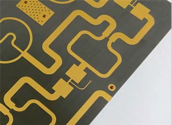
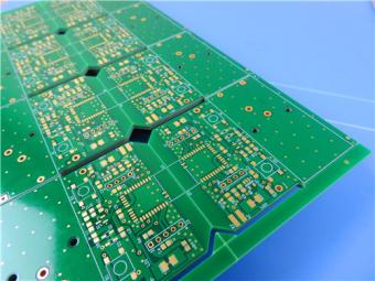
Via Filled PCB Via in Pad Circuit Board 0.6mm Multilayer PCB Built On 6 Layer With Blind Via for GPS Tracking
(Printed circuits boards are custom-made products, the picture and parameters shown are just for reference)
1.1 General description
It's only 0.6 mm thick without silkscreen on green solder mask (Taiyo) and immersion gold on pads. The base material is from Taiwan ITEQ supplying 1 up PCB per panel. Vias with 0.25mm areresin filled and capped (via in pad). They're fabricated per IPC 6012 Class 2 using supplied Gerber data. Each 50 panels are packed for shipment.
1.2 Features and benefits
1. Via in pad design reduced the inductive reactance and capacitive reactance of the transmission line;
2. Immersion gold finish has high solderability, no stressing of circuit boards and less contamination of PCB surface;
3. Products and manufacturing are certified by authorized organizations;
4. Eligible products rate of first production: >95%;
5. Prototype PCB capability to volume production capability;
6. Delivery on time: >98%;
7. More than 18+ years of PCB experience;
8. IPC Class 2 / IPC Class 3;

1.3 Applications
Led Lighting
Intercom System
Portable WiFi Router
GSM Tracker
Commercial Led Lighting
Modem WiFi 4G
Honeywell Access Control
Electronic Access Control
Audio Frequency Amplifier
File servers
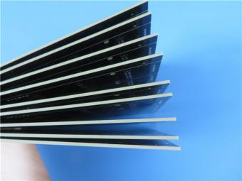
1.4 PCB Specifications
| PCB SIZE | 100 x 103mm=1PCS |
| BOARD TYPE | Multilayer PCB |
| Number of Layers | 6 layers |
| Surface Mount Components | YES |
| Through Hole Components | NO |
| LAYER STACKUP | copper ------- 18um(0.5oz)+plate TOP CS |
| 4mil prepreg | |
| copper ------- 18um(0.5oz) GND Plane | |
| 4mil FR-4 | |
| copper ------- 18um(0.5oz) PWR Plane | |
| 4mil prepreg | |
| copper ------- 18um(0.5oz) PWR Plane | |
| 4mil FR-4 | |
| copper ------- 18um(0.5oz) SIG | |
| 4mil prepreg | |
| copper ------- 18um(0.5oz) BOT PS | |
| TECHNOLOGY | |
| Minimum Trace and Space: | 3mil/3mil |
| Minimum / Maximum Holes: | 0.22/3.50mm |
| Number of Different Holes: | 25 |
| Number of Drill Holes: | 2315 |
| Number of Milled Slots: | 0 |
| Number of Internal Cutouts: | 0 |
| Impedance Control | no |
| BOARD MATERIAL | |
| Glass Epoxy: | FR-4, ITEQ IT140 TG>135, er<5.4 |
| Final foil external: | 1oz |
| Final foil internal: | 0.5oz |
| Final height of PCB: | 0.6mm ±0.1 |
| PLATING AND COATING | |
| Surface Finish | Immersion gold 0.025µm over 3µm Nickel (14.4% area) |
| Solder Mask Apply To: | TOP and Bottom, 12micron Minimum |
| Solder Mask Color: | Green, TAIYO PSR-2000 GT600D |
| Solder Mask Type: | LPSM |
| CONTOUR/CUTTING | Routing |
| MARKING | |
| Side of Component Legend | No silkscreen requried. |
| Colour of Component Legend | No silkscreen requried. |
| Manufacturer Name or Logo: | No silkscreen requried. |
| VIA | Plated through hole(PTH), Blind via and via capping on CS and PS, vias not be visible. |
| FLAMIBILITY RATING | UL 94-V0 Approval MIN. |
| DIMENSION TOLERANCE | |
| Outline dimension: | 0.0059" (0.15mm) |
| Board plating: | 0.0030" (0.076mm) |
| Drill tolerance: | 0.002" (0.05mm) |
| TEST | 100% Electrical Test prior shipment |
| TYPE OF ARTWORK TO BE SUPPLIED | email file, Gerber RS-274-X, PCBDOC etc |
| SERVICE AREA | Worldwide, Globally. |

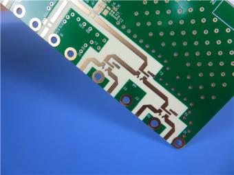
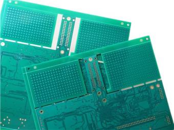
1.5 via in pad (VIP)
At present, the circuit board is becoming more and more dense and interconnected, and there is no more room for these wires and pads connecting the holes. Therefore, so in this context, the process of punching the holes on the pads arises at the historic moment. In brief, the via holes which have been plated through are plugged or filled by insulating resin through the method of screen leakage, and then drying, grinding, and then electroplating, so that the whole surface of the PCB is coated with copper, and no longer via holes can be seen.
The effect of via in pad is also very obvious: such as improved the electrical performance and reliability of electronic products, shorten the signal transmission wire, reduced the inductive reactance and capacitive reactance of the transmission line, and reduced internal and external electromagnetic interference.
Let’s see the basic process of via in pad.

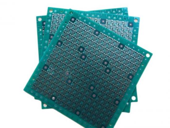
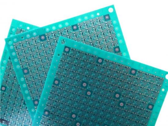
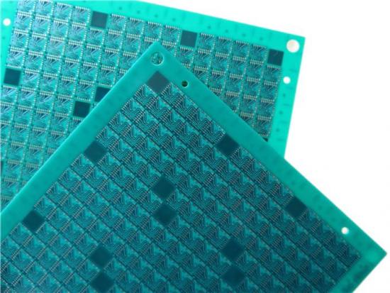
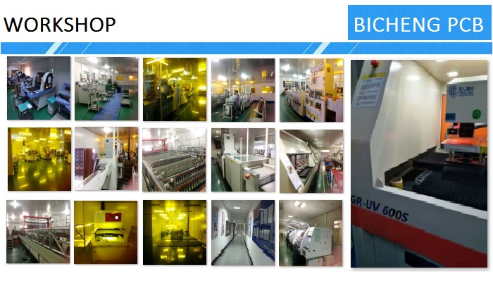
BICHENG PCB WORKSHOP:
BICHENG MAIN COURIERS:

Previous:
PCB Spacer FR-4 Spacer Block Space Bar On 1.5mm FR4 with Drill HolesNext:
Multilayer Printed Circuit Board 8-Layer PCBs Built On Tg175℃ FR-4 With Immersion GoldIf you have questions or suggestions,please leave us a message,we will reply you as soon as we can!
Categories
New Products
Wangling 5mil 0.127mm TFA300 Core 2-layer Immersion Gold Green Solder Mask PCB
7.5mil AGC Taconic TLY-5 Substrate Custom PCB EPIG Finish Bare Copper
10mil Rogers CuClad 250 Immersion Gold 2-Layer Rigid Microwave PCB
20mil F4BTMS450 Wangling DK4.5 Laminate Custom PCB HASL LF Finsh
F4BME275 Wangling DK2.75 Laminate 2-Layer 1.6mm Pure Gold RF Custom PCB
Wangling F4BTD350S High Frequency PCB 2-layer 20mil Thick ENIG DK3.5 Substrate
12-layer TG200 TU-872 SLK High-Speed FR4 1.68mm PCB with ENIG Impedance Control
12-Layer RO4350B + RO3010 3.14mm Hybrid PCB Nickel-Free EPIG Surface Finish Blind Via
Multilayer high frequency PCBs are made from all high frequency material inclusive of prepreg adhesive.
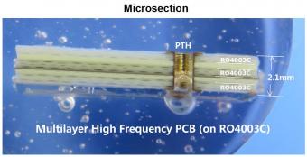
5 layer PCB is fabricated on 3 cores of RO4003C and etched 1 layer copper off to achieve 5 layers.
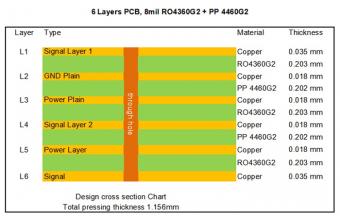
RO4360G2 laminates extend Rogers' portfolio of high performance materials by providing customers with a product that is lead-free process capable and offers better rigidity for improved processability in multi-layer board constructions, while reducing material and fabrication costs.
Megtron 6 is an ultra-low loss, highly heat resistant circuit board material designed for mobile, networking, and wireless applications etc.
This type of 4-layer circuit board is built on Panasonic Megtron6 (M6) R-5775G high speed low loss material.
TU-768 / TU-768P laminate / prepreg are made of high quality woven E-glass coated with the epoxy resin system, which provides the laminates with UV-block characteristic, and compatibility with automated optical inspection (AOI) process.
IT-180ATC is an advanced high Tg (175℃ by DSC) multifunctional filled epoxy with high thermal reliability and CAF resistance.
This is a type of 8-layer printed circuit board built on FR-4 Tg175℃ substrate for the application of Satellite Radio.
 6-11C Shidai Jingyuan, Fuyong, Baoan, Shenzhen, Guangdong, China 518103


For inquiries about our products or pricelist, please leave to us and we will be in touch within 24 hours.
© Copyright: 2026 Shenzhen Bicheng Electronics Technology Co., Ltd.. All Rights Reserved.

IPv6 network supported


