

 Call Us Now !
Tel : +86 755 27374946
Call Us Now !
Tel : +86 755 27374946
 Order Online Now !
Email : info@bichengpcb.com
Order Online Now !
Email : info@bichengpcb.com
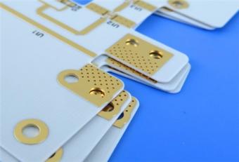
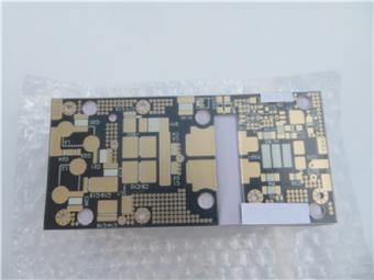
This F4BTMS1000 2-layer PCB is a high-performance radio-frequency and microwave substrate designed for mission-critical applications including aerospace, satellite communications, phased-array antennas, military radar, and high-reliability feed networks.
Item NO.:
BIC-560-v645.0Order(MOQ):
1-10Payment:
T/TProduct Origin:
ChinaShipping Port:
ShenzhenLead Time:
7-10 days
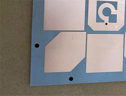
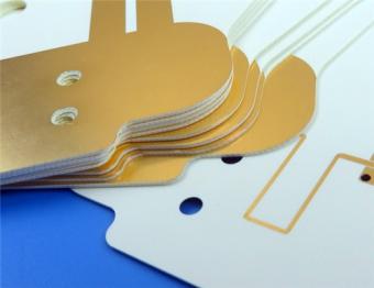
Wangling F4BTMS1000 High DK10.2 Laminate 2-layer 10mil OSP Custom PCB
Overview
This F4BTMS1000 2-layer 10mil OSP PCB is a high-performance radio-frequency and microwave substrate designed for mission-critical applications including aerospace, satellite communications, phased-array antennas, military radar, and high-reliability feed networks. Built on advanced ceramic-filled PTFE composite laminate with ultra-thin ultra-fine fiberglass reinforcement, the board delivers exceptional dielectric stability, low insertion loss, excellent thermal management, and outstanding dimensional consistency under extreme thermal and environmental conditions.
Compliant with IPC-Class-2 quality standards and fully tested for electrical performance, this high DK10.2 F4B PCB provides a dependable, domestically engineered alternative to imported high-DK microwave substrates while maintaining superior process compatibility and mechanical robustness.
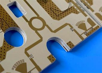
1. PCB Construction
This section summarizes the mechanical, electrical, and surface-finish specifications of the finished PCB, defining its manufacturability, reliability, and application suitability.
|
Parameter |
Value |
|
Base Material |
F4BTMS1000 |
|
Layer Count |
2 layers |
|
Board Dimensions |
79.6 mm × 45 mm (±0.15 mm) |
|
Minimum Trace / Space |
5 / 6 mils |
|
Minimum Finished Hole Size |
0.2 mm |
|
Blind Vias |
Not applicable |
|
Finished Board Thickness |
0.4 mm |
|
Finished Copper Weight (Outer Layers) |
1 oz (≈1.4 mils / 35 μm) |
|
Via Plating Thickness |
20 μm |
|
Surface Finish |
OSP (Organic Solderability Preservative) |
|
Top Silkscreen |
None |
|
Bottom Silkscreen |
None |
|
Top Solder Mask |
None |
|
Bottom Solder Mask |
None |
|
Electrical Test |
100% full electrical test before shipment |
2. PCB Stackup
The stackup defines the layer structure, copper thickness, and dielectric core configuration, directly influencing impedance control, signal integrity, and mechanical stability.
|
Layer |
Material |
Thickness |
|
Copper Layer 1 (Top) |
1 oz RTF low-roughness copper foil |
35 μm |
|
Dielectric Core |
F4BTMS1000 |
0.254 mm (10 mil) |
|
Copper Layer 2 (Bottom) |
1 oz RTF low-roughness copper foil |
35 μm |
|
Total Finished Board Thickness |
— |
0.4 mm |
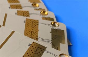
3. PCB Layout Statistics
This table quantifies component, pad, via, and net density, supporting assembly feasibility, routing efficiency, and thermal analysis.
|
Item |
Quantity |
|
Component Count |
42 |
|
Total Pads |
78 |
|
Through-Hole Pads |
41 |
|
Top SMT Pads |
37 |
|
Bottom SMT Pads |
0 |
|
Vias |
36 |
|
Nets |
2 |
Product Performance & Differentiators
F4BTMS1000 represents an upgraded formulation of the F4BTM laminate series, engineered with nano-scale ceramic fillers and ultra-thin ultra-fine fiberglass cloth to minimize glass-weave effects, reduce dielectric anisotropy, and improve high-frequency signal transparency. Unlike standard FR-4 or mid-grade microwave materials, this F4B DK10.2 substrate maintains stable electrical properties across wide temperature and frequency ranges, making it ideal for phase-sensitive systems such as phased-array antennas and satellite feeds.

Key advantages include:
1)Ultra-low dissipation factor: Df = 0.0020 at 10 GHz, supporting low insertion loss in high-frequency RF paths.
2)Stable dielectric constant: Dk = 10.2 at 10 GHz with tight tolerance, enabling precise impedance matching and miniaturized circuit designs.
3)Low thermal coefficient of Dk:−320 ppm/°C from−55°C to 150°C, ensuring phase stability over extreme thermal cycles.
4)Balanced CTE performance: CTE x = 16 ppm/°C, y = 18 ppm/°C, z = 32 ppm/°C (−55°C to 288°C), reducing thermal stress and improving via reliability.
5)High thermal conductivity: 0.81 W/m·K, supporting higher power density and improved heat dissipation.
6)Near-zero moisture absorption: 0.03%, preserving electrical stability in high-humidity environments.
7)RTF low-roughness copper foil: Reduces conductor loss at high frequencies while providing strong peel strength (>1.2 N/mm).
8)Excellent process compatibility: Supports fine lines, small vias, and dense routing without sacrificing yield or reliability.
Absence of solder mask and silkscreen preserves high-frequency performance by eliminating additional dielectric loading and surface roughness, making this board optimized for bare-copper RF circuits, microwave probes, and high-altitude or vacuum environments. OSP surface protection preserves solderability while maintaining a clean, low-loss contact interface.
This F4BTMS1000 high frequency PCB is fully qualified for aerospace and space-borne equipment, military radar systems, satellite communication payloads, and high-performance microwave modules. It serves as a high-reliability domestic alternative to imported high-DK ceramic-filled PTFE materials, delivering consistent performance with shorter lead times and stronger supply chain stability.
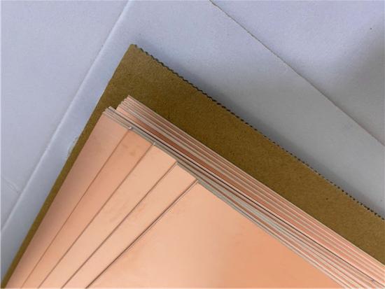
Part 2: CCL (Copper Clad Laminate) Technical Overview–F4BTMS1000
This section provides an in-depth explanation of the copper clad laminate used in the above PCB, including material composition, full datasheet specifications, structural advantages, and application guidance.
What is F4BTMS1000 CCL?
F4BTMS1000 is a high-performance ceramic-filled PTFE copper clad laminate designed specifically for microwave, RF, and high-frequency applications up to 40 GHz. It is an upgraded version of the F4BTM series, formulated with uniformly dispersed nano-ceramic particles and reinforced with ultra-thin ultra-fine fiberglass cloth to minimize dielectric loss, reduce anisotropy, enhance dimensional stability, and improve thermal conductivity. As an aerospace-grade base material, it offers a dependable replacement for foreign high-DK microwave substrates while supporting standard PTFE PCB processing flows.

Core Composition
Full CCL Datasheet–F4BTMS1000
All values are typical tested data in accordance with IPC-TM-650 and GB/T standards.
|
Parameter |
Test Condition |
Unit |
Typical Value |
|
Dielectric Constant (Dk) |
10 GHz |
— |
10.2 |
|
Dk Tolerance |
10 GHz |
— |
±0.2 |
|
Dissipation Factor (Df) |
2 GHz |
— |
0.002 |
|
Dissipation Factor (Df) |
10 GHz |
— |
0.0023 |
|
Thermal Coefficient of Dk |
−55°C to 150°C |
ppm/°C |
−320 |
|
Peel Strength |
1 oz RTF copper |
N/mm |
>1.2 |
|
Volume Resistivity |
Normal condition |
MΩ·cm |
≥1×10⁸ |
|
Surface Resistance |
Normal condition |
MΩ |
≥1×10⁸ |
|
Dielectric Strength (Z-axis) |
5 mm, 500 V/s |
kV/mm |
>23 |
|
Breakdown Voltage (XY-plane) |
5 mm, 500 V/s |
kV |
>42 |
|
CTE (X-axis) |
−55°C to 288°C |
ppm/°C |
16 |
|
CTE (Y-axis) |
−55°C to 288°C |
ppm/°C |
18 |
|
CTE (Z-axis) |
−55°C to 288°C |
ppm/°C |
32 |
|
Thermal Stress Resistance |
260°C, 10 s, 3 cycles |
— |
No delamination |
|
Moisture Absorption |
20±2°C, 24 h |
% |
0.03 |
|
Density |
Room temperature |
g/cm³ |
3.2 |
|
Continuous Use Temperature |
Thermal chamber |
°C |
−55 to +260 |
|
Thermal Conductivity (Zaxis) |
— |
W/(m·K) |
0.81 |
|
Flammability |
UL94 |
— |
V-0 |
Key CCL Advantages
1)Low dielectric loss and stable Dk
Optimized for phase-sensitive systems, the material maintains consistent electrical performance across temperature and frequency, ensuring signal fidelity in radar and satellite links.
2)Minimized anisotropy
Ultra-thin fiberglass and uniform ceramic distribution reduce X/Y/Z anisotropy, lowering beam-squint and phase errors in array antennas.
3)Excellent thermal stability
Low CTE and high thermal conductivity improve reliability under thermal cycling and high-power operation.
4)Ultra-low moisture absorption
Near-zero water uptake preserves electrical performance in high-altitude, humid, or vacuum environments.
5)Strong adhesion and low conductor loss
Standard RTF low-roughness copper reduces skin-effect loss while maintaining high peel strength.
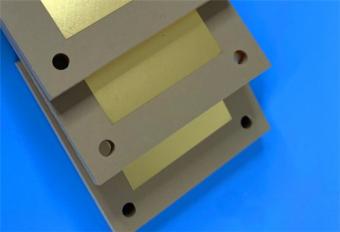
6)Metal-backed options available
F4BTMS1000-AL (aluminum base) and F4BTMS1000-CU (copper base) versions provide integrated shielding and enhanced thermal dissipation.
Typical Applications of F4BTMS1000 CCL
-Aerospace and satellite payloads
-Military and civilian radar systems
-Phased-array antennas and phase-sensitive feeds
-Microwave and RF transceivers
-5G/6G high-frequency components
-Space and cabin electronic equipment
-High-power microwave modules
Ordering Information for CCL
Fabrication Guidelines for F4BTMS1000
1) Drilling: Use carbide drills with pecking cycles; PTFE tends to smear. Plasma or sodium etching may be required for through-hole wetting prior to electroless copper.
2) Handling: Soft material; avoid scratching.
3) Registration: Low X/Y expansion allows standard tooling, but thin cores (0.254 mm) require careful lamination pressure control.
4) Surface Finish: OSP, ENIG, or Immersion Silver are compatible. HASL not recommended due to high thermal shock
Conclusion
The F4BTMS1000 2-layer PCB with OSP finish leverages the full capabilities of its advanced CCL substrate. With a finished thickness of just 0.4 mm, fine 5/6 mil trace/space, and 20μm via plating, this board is built for high-frequency reliability. The underlying F4BTMS1000 laminate provides a stable Dk of 10.2, ultra-low loss of 0.0020, excellent CTE matching, and thermal conductivity nearly triple that of conventional PTFE. Whether deployed in a space satellite, military radar, or 5G infrastructure feed network, this Wangling PCB delivers measurable, repeatable performance—backed by full electrical test and IPC-Class-2 compliance.
For engineers seeking a compact, phase-stable, and thermally resilient RF board, this F4BTMS1000-based design represents a technically sound, manufacturing-ready solution.


If you have questions or suggestions,please leave us a message,we will reply you as soon as we can!
Categories
New Products
RO4835 20mil Rogers Laminate 2-layer Immersion Gold Custom PCB
Rogers 20mil DiClad 527 PCB 2-layer Immersion Gold No Solder Mask Black Silkscreen
Wangling WL-CT300 5mil Laminate Pure Gold Plating High Frequency PCB
Wangling TF300 25mil DK3.0 Laminate 2-layer PCB Immersion Gold Black Silkscreen
2-Layer 0.5mm TP440 PCB Wangling TP DK4.4 Laminate Immersion Gold
20-Layer Panasonic TU872 HDI PCB ENEPIG 3.0mm Finished Thick Laser-drilled Blind Vias
10-Layer Rogers RO4003C + 370HR FR4 Hybrid Laminate PCB ENIG Impedance Control
8-Layer 10oz Heavy Copper TU-865 Substrate PCB With ENIG Blind &Buried Via
F4B series high frequency material is mainly PTFE glass fiber cloth and ceramic-filled PTFE glass fiber cloth etc. It is a series of high frequency materials of Chinese brand, which is cheap in price and stable in quality.
Metal based substrate is a combination of metal based high frequency materials. The intermediate medium is made of high frequency materials, one side is coated with copper foil, the other side is coated with copper base or aluminum base.
PTFE commonly known as "plastic king ", is a polymer compound made of tetrafluoroethylene by polymerization. It has excellent chemical stability, corrosion resistance, sealing, high lubrication and non-viscosity, electrical insulation and good aging resistance.
PTFE has excellent chemical stability, corrosion resistance, sealing, high lubrication and non-viscosity, electrical insulation and good aging resistance. Used as engineering plastic, it can be made into PTFE tube, rod, belt, plate, film and so on.
RF-60TC is by improving dielectric heat dissipation and exceptionally lower dielectric losses, a better gain and efficiency are got in miniaturized antenna applications.

F4B is laminated by laying up of varnished glass cloth with Teflon resin, according to the scientific formulation and strict technology process. This product takes some advantages over F4B series in the electrical performance(wider range of dielectric constant).
F4B is a series of PTFE based high frequency materials which is brand of China.
This 2-Layer Aluminum Core PCB is more than a component; it is a thermal management system engineered onto a board.
 6-11C Shidai Jingyuan, Fuyong, Baoan, Shenzhen, Guangdong, China 518103


For inquiries about our products or pricelist, please leave to us and we will be in touch within 24 hours.
© Copyright: 2026 Shenzhen Bicheng Electronics Technology Co., Ltd.. All Rights Reserved.

IPv6 network supported


