

 Call Us Now !
Tel : +86 755 27374946
Call Us Now !
Tel : +86 755 27374946
 Order Online Now !
Email : info@bichengpcb.com
Order Online Now !
Email : info@bichengpcb.com
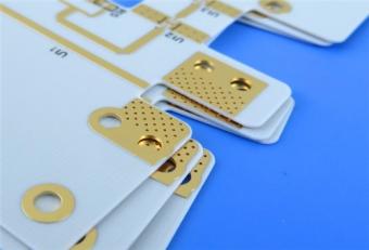
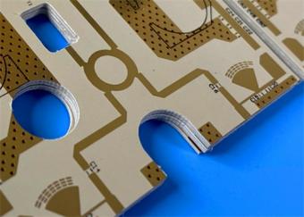
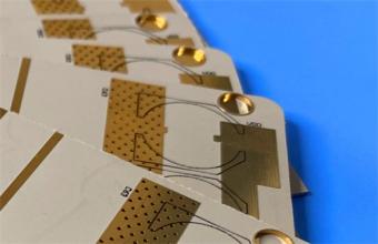
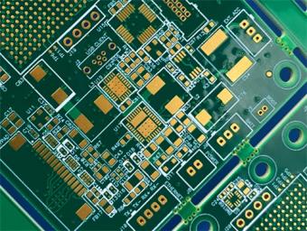
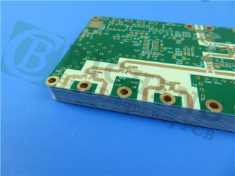
This F4BME217 2-layer PCB integrates advanced PTFE composite material, RTF copper, precision fabrication, and IPC-Class-2 quality to create a high-performance, cost-effective solution for professional RF and microwave systems.
Item NO.:
BIC-559-v644.0Order(MOQ):
1-10Payment:
T/TProduct Origin:
ChinaShipping Port:
ShenzhenLead Time:
7-10 days
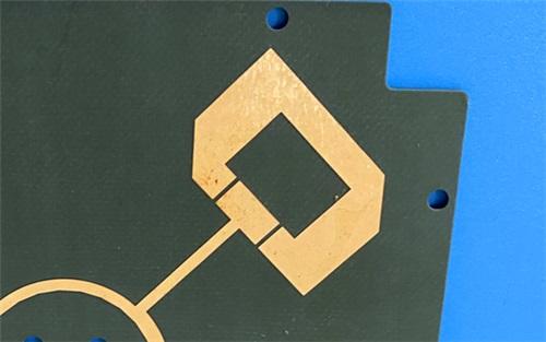
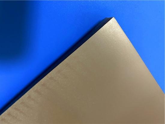
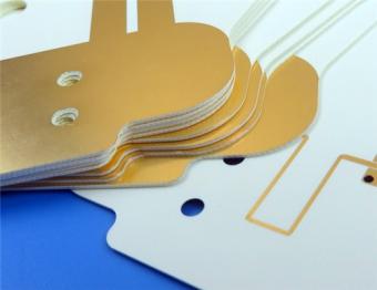
Wangling F4BME217 PCB 1mm Thick DK2.17 Substrate 2-Layer Bare Copper
1. Product Overview
This is a high-performance 2-layer RF/microwave printed circuit board built on Wangling F4BME217 PTFE composite laminate, with a nominal dielectric core thickness of 1.0 mm and finished board thickness of 1.3 mm. It adopts bare copper surface treatment, no solder mask or silkscreen, and is manufactured to IPC-Class-2 quality standards with 100% electrical testing before shipment. The DK2.17 F4B PCB is purpose-engineered for high-frequency, low-loss, high-stability RF systems such as microwave links, radar front-ends, passive components, antenna feed networks, satellite communication, and 5G base station antennas. It delivers excellent passive intermodulation (PIM) performance, fine-line etching capability, and low conductor loss, serving as a reliable domestic alternative to imported high-frequency RF PCBs.

2. PCB Construction
This section summarizes the mechanical, fabrication, and surface finishing specifications of the finished PCB, covering outline dimensions, line/space capability, hole size, copper weight, surface treatment, and quality control.
|
Item |
Specification |
|
Board Type |
2-layer rigid RF PCB |
|
Board Dimensions |
102 mm × 83 mm (1 piece), tolerance ±0.15 mm |
|
Minimum Trace / Space |
5 / 6 mils |
|
Minimum Finished Hole Size |
0.25 mm |
|
Finished Board Thickness |
1.3 mm |
|
Finished Copper Weight (Outer Layers) |
1 oz (1.4 mils, ~35 μm) |
|
Via Plating Thickness |
20 μm |
|
Surface Finish |
Bare copper |
|
Top Silkscreen |
No |
|
Bottom Silkscreen |
No |
|
Top Solder Mask |
No |
|
Bottom Solder Mask |
No |
|
Quality Standard |
IPC-Class-2 |
|
Pre shipment Test |
100% electrical test |
3. PCB Stackup & Layer Structure
The stackup defines the layer sequence and thickness distribution, ensuring impedance control, mechanical stability, and low-loss high-frequency transmission.
|
Layer |
Material |
Thickness |
|
Copper Layer 1 (Top) |
Electrodeposited / Reverse Treated Foil (RTF) |
35 μm |
|
Core Dielectric |
F4BME217 PTFE composite |
1.0 mm (39.37 mils) |
|
Copper Layer 2 (Bottom) |
Electrodeposited / Reverse Treated Foil (RTF) |
35 μm |
|
Total Finished Thickness |
— |
1.3 mm |
4. PCB Layout Statistics Summary & Design Data
This table provides key layout metrics for assembly planning, impedance design, and process verification.
|
Item |
Quantity |
|
Component Count |
15 |
|
Total Pads |
42 |
|
Through hole Pads |
17 |
|
Top SMT Pads |
25 |
|
Bottom SMT Pads |
0 |
|
Vias |
28 |
|
Nets |
7 |
5. Core Performance Advantages & Differentiators
5.1 Low Dielectric Loss & High-Frequency Stability
Wangling F4BME217 is a woven fiberglass-reinforced PTFE composite optimized for RF and microwave use. At 10 GHz, its typical dielectric constant Dk = 2.17 (tolerance±0.04) and dissipation factor Df = 0.001; at 20 GHz, Df = 0.0014, enabling extremely low insertion loss and stable phase response across wide bandwidths.
5.2 Superior PIM & Low Conductor Loss
F4BME217 high frequency PCB uses Reverse-Treated Foil (RTF) copper, which greatly improves low-PIM performance, supports finer circuit etching, and reduces conductor loss compared with standard ED foil. This is critical for high-sensitivity receivers, multicarrier power amplifiers, and antenna arrays.
5.3 Excellent Dimensional & Thermal Stability
By balancing PTFE and fiberglass ratio, the material achieves controllable Dk, low loss, and enhanced dimensional stability. Higher fiberglass content increases Dk, lowers CTE, reduces temperature drift, and improves reliability under thermal cycling.
5.4 Bare Copper Structure for RF Performance
Bare copper finish eliminates signal attenuation from surface finishes like ENIG or HASL. The absence of solder mask and silkscreen preserves consistent dielectric environment, reduces parasitic effects, and supports optimal high-frequency performance.
5.5 High Insulation & Voltage Withstand
Volume resistivity≥6×10⁶MΩ·cm, surface resistivity≥1×10⁶MΩ, electrical strength >23 kV/mm, and breakdown voltage >30 kV ensure safe operation in high-voltage RF bias circuits.
5.6 Wide Temperature & Environmental Resistance
Long-term working temperature:−55°C to +260°C. Passes 260°C, 10 s, 3 cycles thermal stress without delamination. Water absorption≤0.08%, making it suitable for outdoor, aerospace, and harsh industrial environments.
6. Typical Target Applications
Part 2: CCL (Copper Clad Laminate) Technical Knowledge
1. Introduction to F4BME217 CCL
F4BME217 is a high-performance PTFE-based copper clad laminate developed by Taizhou Wangling Insulation Materials Factory for RF, microwave, and millimeter-wave applications. It combines woven fiberglass cloth, PTFE resin, and film to deliver stable electrical properties, low loss, and good mechanical strength. It outperforms legacy F4B220 with lower loss, higher insulation resistance, and better stability, and serves as a cost-effective domestic substitute for imported high-frequency laminates.
2. Full Datasheet Parameters of F4BME217 CCL
|
Parameter |
Test Condition |
Unit |
Typical Value |
|
Dielectric Constant (Dk) |
10 GHz |
— |
2.17 |
|
Dk Tolerance |
— |
— |
±0.04 |
|
Dissipation Factor (Df) |
10 GHz |
— |
0.001 |
|
Dissipation Factor (Df) |
20 GHz |
— |
0.0014 |
|
Temperature Coefficient of Dk |
−55°C ~ 150°C |
ppm/°C |
−150 |
|
Peel Strength (F4BME / RTF) |
1 oz foil |
N/mm |
>1.6 |
|
Volume Resistivity |
Normal |
MΩ·cm |
≥6×10⁶ |
|
Surface Resistance |
Normal |
MΩ |
≥1×10⁶ |
|
Electrical Strength (Z-axis) |
5 kV, 500 V/s |
kV/mm |
>23 |
|
Breakdown Voltage (XY-plane) |
5 kV, 500 V/s |
kV |
>30 |
|
CTE (XY-direction) |
−55°C ~ 288°C |
ppm/°C |
25–34 |
|
CTE (Z-direction) |
−55°C ~ 288°C |
ppm/°C |
240 |
|
Thermal Stress |
260°C, 10 s, 3 cycles |
— |
No delamination |
|
Water Absorption |
20±2°C, 24 h |
% |
≤0.08 |
|
Density |
Normal |
g/cm³ |
2.17 |
|
Long-Term Operating Temp |
— |
°C |
−55 ~ +260 |
|
Thermal Conductivity (Z-axis) |
— |
W/(m·K) |
0.24 |
|
Passive Intermodulation (PIM) |
F4BME series only |
dBc |
≤−159 |
|
Flammability |
UL-94 |
— |
V-0 |
|
Material Composition |
— |
— |
PTFE + fiberglass cloth; RTF copper foil |

3. Key Technical Features of F4BME217 CCL
3.1 Customizable Dielectric Properties
Dk ranges from 2.17 to 3.0 and can be customized by adjusting PTFE-to-fiberglass ratio. Higher Dk improves dimensional stability and lowers CTE but slightly increases Df, allowing engineers to balance electrical performance, mechanical robustness, and processing needs.
3.2 F4BM vs. F4BME vs. F4BME217
3.3 Copper Foil Options
RTF provides better surface roughness control, improved adhesion, and superior high-frequency performance.
3.4 Available Sizes & Thicknesses
3.5 Metal-Backed Versions (Al/Cu Base)
4. Why F4BME217 Stands Out in RF/Microwave CCL
5. Testing & Compliance
Dk/Df: GB/T 12636-1990, IPC-TM-650 2.5.5.5 stripline method
Other properties: IPC-TM-650, GB/T 4722-2017
All data are typical values for material selection; customers should verify suitability for specific applications.
6.Conclusion
This F4BME217 1mm 2-layer PCB integrates advanced PTFE composite material, RTF copper, precision fabrication, and IPC-Class-2 quality to create a high-performance, cost-effective solution for professional RF and microwave systems. Its low loss, low PIM, stable Dk, and mechanical robustness make it suitable for commercial and industrial communication systems while avoiding overspecification and unnecessary cost. Supported by complete CCL engineering data and scalable manufacturing, this platform supports reliable mass production and consistent field performance.


Previous:
2-Layer RO4350B LoPro PCB 4mil Rogers Substrate Immersion Gold Blue Solder MaskNext:
Rogers CLTE-MW PCB 2.9mil 2-layer Immersion Gold No Solder Mask Black SilkscreenIf you have questions or suggestions,please leave us a message,we will reply you as soon as we can!
Categories
New Products
RO4835 20mil Rogers Laminate 2-layer Immersion Gold Custom PCB
Rogers 20mil DiClad 527 PCB 2-layer Immersion Gold No Solder Mask Black Silkscreen
Wangling WL-CT300 5mil Laminate Pure Gold Plating High Frequency PCB
Wangling TF300 25mil DK3.0 Laminate 2-layer PCB Immersion Gold Black Silkscreen
2-Layer 0.5mm TP440 PCB Wangling TP DK4.4 Laminate Immersion Gold
20-Layer Panasonic TU872 HDI PCB ENEPIG 3.0mm Finished Thick Laser-drilled Blind Vias
10-Layer Rogers RO4003C + 370HR FR4 Hybrid Laminate PCB ENIG Impedance Control
8-Layer 10oz Heavy Copper TU-865 Substrate PCB With ENIG Blind &Buried Via
This is a type of double sided RF PCB built on RT/duroid 5880 for the application of Radar Systems.
RO4003C PCBs are hydrocarbon ceramic filled laminates, not PTFE which are designed to offer superior high frequency performance.
Rogers RO3003 high frequency circuit materials are ceramic-filled PTFE composites intended for use in commercial microwave and RF applications. It was designed to offer exceptional electrical and mechanical stability at competitive prices.
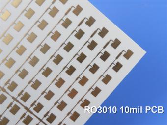
RO3010 laminates are competitively priced products with exceptional mechanical and electrical stability. This stability simplifies the design of broadband components and allows the materials to be used in a wide range of applications over a very broad range of frequencies.
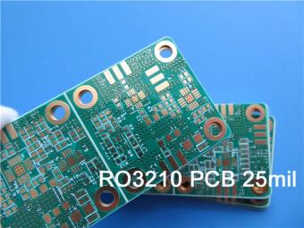
These RO3210 materials are engineered to offer exceptional electrical performance and mechanical stability. RO3210 laminates combine the surface smoothness of a non-woven PTFE laminate.
RT/duroid 6035HTC laminates are an exceptional choice for high power applications.
TC350 is designed to provide enhanced heat-transfer through “Best-In-Class” thermal conductivity, while reducing dielectric loss and insertion loss. Lower losses result in higher Amplifier and Antenna Gains/Efficiencies.
RO3035 materials exhibit a coefficient of thermal expansion(CTE) in the X and Y axis of 17 ppm/℃. This expansion coefficient is matched to that of copper, which allows the material to exhibit excellent dimensional stability.
 6-11C Shidai Jingyuan, Fuyong, Baoan, Shenzhen, Guangdong, China 518103


For inquiries about our products or pricelist, please leave to us and we will be in touch within 24 hours.
© Copyright: 2026 Shenzhen Bicheng Electronics Technology Co., Ltd.. All Rights Reserved.

IPv6 network supported


