

 Call Us Now !
Tel : +86 755 27374946
Call Us Now !
Tel : +86 755 27374946
 Order Online Now !
Email : info@bichengpcb.com
Order Online Now !
Email : info@bichengpcb.com
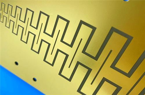
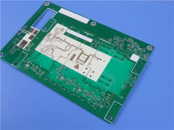
This 2-Layer RF-10 PCB is specifically engineered for size-sensitive, high-performance RF circuits where signal integrity, thermal management, and dimensional stability are paramount.
Item NO.:
BIC-557-v642.0Order(MOQ):
1-10Payment:
T/TProduct Origin:
ChinaShipping Port:
ShenzhenLead Time:
7-10 days
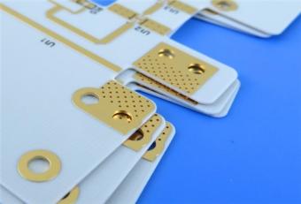
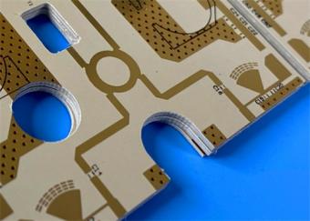
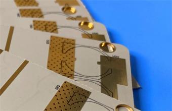
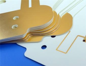
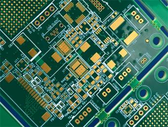
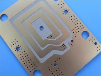
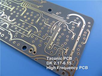
2-Layer RF-10 AGC Taconic High FrequencyPCB 10mil ENEPIG DK10.2 Laminate
Introduction
In the demanding world of high-frequency RF and microwave applications, substrate material selection and PCB construction quality directly dictate system performance. This 2-Layer RF-10 PCB is specifically engineered for size-sensitive, high-performance RF circuits where signal integrity, thermal management, and dimensional stability are paramount. By combining a ceramic-filled PTFE composite core (RF-10) with a premium ENEPIG surface finish, this Taconic PCB board delivers consistent electrical performance, excellent solderability, and long-term reliability in harsh environments.
Unlike conventional FR-4 designs, this 10mil RF-10 PCB leverages ahigh dielectric constant (Dk = 10.2) to reduce circuit footprint without compromising electromagnetic performance. The 10mil (0.254mm) core thickness and 1oz copper outer layers enable tight impedance control, while the absence of solder mask and silkscreen minimizes parasitic losses—critical for millimeter-wave and microstrip applications.

1. PCB Construction Details
This section summarizes the physical manufacturing specifications, surface treatment, and quality control parameters that define the board’s mechanical and assembly-ready characteristics.
|
Parameter |
Value |
|
Board Dimensions |
143.6mm × 109.8mm (2 types, 2 PCS), tolerance ±0.15mm |
|
Minimum Trace / Space |
5 / 7 mils |
|
Minimum Hole Size |
0.4mm |
|
Blind Vias |
Not applicable |
|
Finished Board Thickness |
0.5mm |
|
Finished Copper Weight (Outer Layers) |
1oz (1.4 mils, 35μm) |
|
Via Plating Thickness |
20μm |
|
Surface Finish |
ENEPIG (Electroless Nickel Electroless Palladium Immersion Gold) |
|
Top Silkscreen |
No |
|
Bottom Silkscreen |
No |
|
Top Solder Mask |
No |
|
Bottom Solder Mask |
No |
|
Pre-Shipment Test |
100% Electrical test |
2. PCB Stackup
This stackup defines the layer structure and material thickness of the rigid 2-layer RF-10 PCB, ensuring stable dielectric performance and mechanical strength.
|
Layer |
Material & Thickness |
|
Copper Layer 1 (Outer) |
35μm (1oz) |
|
Core Dielectric |
RF-10, 10mil (0.254mm) |
|
Copper Layer 2 (Outer) |
35μm (1oz) |
3. PCB Statistics
This table summarizes the circuit layout density, component interconnection, and electrical network configuration of the finished PCB.
|
Item |
Quantity |
|
Components |
24 |
|
Total Pads |
51 |
|
Thru-Hole Pads |
34 |
|
Top SMT Pads |
17 |
|
Bottom SMT Pads |
0 |
|
Vias |
29 |
|
Nets |
2 |
PCB Design, Manufacturing & Performance Advantages
This Taconic RF-10 PCB is engineered for high-frequency signal integrity, miniaturized form factors, and long-term operational stability—key differentiators in competitive RF hardware markets.
1)Ultra-Thin, High-Stability Mechanical Design
With a finished thickness of only 0.5mm, the board achieves exceptional compactness while maintaining structural rigidity. The10mil RF-10 core delivers a high dielectric constant (Dk=10.2±0.3@10GHz), enabling significant circuit size reduction compared to standard PTFE or hydrocarbon substrates. This is critical for space-constrained platforms such as small antennas, portable GPS receivers, and satellite payloads. The absence of blind vias simplifies manufacturing, lowers cost, and improves via-plating integrity, while the 20μm via plating ensures robust electrical conductivity and thermal fatigue resistance across temperature cycles.
2)ENEPIG Surface Finish for RF Excellence
ENEPIG is selected over conventional finishes (ENIG, HASL, Immersion Silver) for its superior high-frequency and reliability traits:
Differentiation & Market Positioning
This RF-10 Taconic High Frequency PCB stands apart from generic high-frequency boards through five core differentiators:
1)Material-Signal Synergy: RF-10’s low dissipation factor (0.0025@10GHz) paired with smooth copper and solder-mask-free construction delivers best-in-class insertion loss for high-frequency links.
2)Thermal Robustness: 0.85W/m·K thermal conductivity and low CTE (X:16, Y:20, Z:25ppm/°C) reduce thermal stress and improve heat dissipation for high-power RF circuits.
3)Miniaturization Enablement: High Dk allows 30–50% smaller circuit footprints vs. standard Dk=2–6 substrates, critical for compact aerospace and satellite designs.
4)Manufacturing Replicability: Compatible with standard PTFE processing (drilling, milling, plating) ensures stable yields, consistent quality, and competitive lead times.
5)Balanced Cost-Performance: Premium RF performance without exotic pricing, making it ideal for volume applications in antennas, filters, and radar systems.
Applications
Given its construction and material set, this Taconic RF PCB Circuit Board is ideally suited for:
RF-10 Copper Clad Laminate (CCL)–Complete Material Knowledge Base
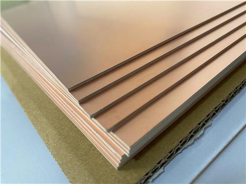
RF-10 substrate is a high-performance ceramic-filled PTFE composite laminate reinforced with woven fiberglass, developed by AGC for high-power and high-frequency RF applications. It combines a high dielectric constant, ultra-low dissipation factor, excellent thermal conductivity, and low thermal expansion—filling the market demand for miniaturized, stable, and cost-effective RF substrates. It supports standard PTFE PCB processing (shearing, drilling, milling, plating) and bonds strongly to smooth low-profile copper, minimizing insertion loss at high frequencies where skin-effect loss dominates. This section provides full material parameters, characteristics, and processing guidelines to support material selection and reliability analysis.
Full RF-10 CCL Datasheet
|
Property |
Conditions |
Typical Value |
Unit |
Test Method |
|
Dielectric Constant |
@ 10 GHz |
10.2 ± 0.3 |
— |
IPC-650 2.5.5.5.1 Mod. |
|
Dissipation Factor |
@ 10 GHz |
0.0025 |
— |
IPC-650 2.5.5.5.1 Mod. |
|
Surface Resistivity |
— |
1.0 × 10⁸ |
Mohms |
IPC-650 2.5.17.1 |
|
Volume Resistivity |
— |
6.0 × 10⁷ |
Mohms/cm |
IPC-650 2.5.17.1 |
|
Thermal Conductivity |
Unclad |
0.85 |
W/m·K |
IPC-650-2.4.50 |
|
CTE (RT-150°C) – X |
— |
16 |
ppm/°C |
IPC-650 2.4.41 |
|
CTE (RT-150°C) – Y |
— |
20 |
ppm/°C |
IPC-650 2.4.41 |
|
CTE (RT-150°C) – Z |
— |
25 |
ppm/°C |
IPC-650 2.4.41 |
|
TcK† (-55 to 150°C) |
— |
-370 |
ppm/°C |
IPC-650 2.5.5.6 |
|
Flexural Strength – MD |
— |
96.53 (14,000) |
N/mm² (psi) |
IPC-650-2.4.4 |
|
Flexural Strength – CD |
— |
68.95 (10,000) |
N/mm² (psi) |
IPC-650-2.4.4 |
|
Tensile Strength – MD |
— |
62.57 (8,900) |
N/mm² (psi) |
IPC-650-2.4.19 |
|
Tensile Strength – CD |
— |
37.26 (5,300) |
N/mm² (psi) |
IPC-650-2.4.19 |
|
Dimensional Stability (25 mil, after etch) – MD |
— |
-0.0032 |
% |
IPC-650 2.4.39 |
|
Dimensional Stability (25 mil, after etch) – CD |
— |
-0.0239 |
% |
IPC-650 2.4.39 |
|
Moisture Absorption |
— |
0.08 |
% |
IPC-650 2.6.2.1 |
|
Peel Strength (1 oz, RT copper) |
— |
1.7 |
N/mm |
IPC-650 2.4.8 (solder) |
|
Density |
Specific gravity |
2.77 |
g/cm³ |
IPC-650-2.3.5 |
|
Specific Heat |
— |
0.9 |
J/g·°C |
IPC-650-2.4.50 |
|
Flammability Rating |
— |
V-0 |
— |
Internal |

Core Characteristics of RF-10 CCL
1)High & Stable Dielectric Constant
Dk=10.2±0.3@10GHz with tight tolerance enables significant RF circuit size reduction—ideal for compact antennas and satellite components where space is limited. Dk remains stable across frequency and temperature, ensuring consistent impedance and signal propagation.
2)Ultra-Low Dissipation Factor
Df=0.0025@10GHz minimizes signal attenuation and energy loss as heat, supporting high-efficiency power transmission and long-distance signal integrity in microwave/RF systems.
3)Excellent Thermal Management
Thermal conductivity of 0.85W/m·K (unclad) improves heat dissipation, preventing thermal drift and performance degradation in high-power RF modules.
4)Low Thermal Expansion (CTE)
X:16, Y:20, Z:25ppm/°C reduce thermal stress on vias and solder joints, enhancing plated through-hole reliability and reducing artwork compensation scaling factors.
5)High Dimensional Stability & Low Moisture Absorption
Low shrinkage/deformation after etching, baking, and stress ensures consistent circuit geometry. Moisture absorption of only 0.08% guarantees stable performance in high-humidity aerospace and satellite environments.
6)Good Process Compatibility
Compatible with standard PTFE PCB fabrication processes; strong adhesion to smooth copper optimizes high-frequency performance by reducing skin-effect loss.
Available Thicknesses
RF-10 laminate can be manufactured in 0.005" (0.125mm) increments. Common thicknesses include:
|
Inches |
mm |
|
0.01 |
0.25 |
|
0.02 |
0.51 |
|
0.025 |
0.64 |
|
0.06 |
1.52 |
|
0.1 |
2.54 |
|
0.125 |
3.18 |
Standard Panel Sizes
|
Inches |
mm |
|
12 × 18 |
305 × 457 |
|
16 × 18 |
406 × 457 |
|
18 × 24 |
457 × 610 |
|
36 × 48 |
914 × 1220 |
Standard panel size: 18"×24". Custom sizes available upon request.
Typical Applications of RF-10 CCL
Processing Guidelines
RF-10 Taconic PCB Laminates can be processed using standard PTFE circuit board techniques:
1)Shearing & Drilling–Standard carbide tools. No special coolant required.
2)Plating–Sodium naphthalate etch or plasma treatment recommended prior to electroless copper deposition.
3)Lamination–Use low-flow prepreg with controlled cooling to prevent warp.
Conclusion
This 2-layer 10mil RF-10 PCB with ENEPIG finish is a high-performance, application-optimized solution that integrates advanced material properties, precision manufacturing, and high-frequency-oriented design. The PCB’s zero-coating structure, ENEPIG surface treatment, and strict quality control ensure exceptional signal integrity and reliability in demanding RF environments. The accompanying RF-10 Taconic RF Laminates provides a complete data set of electrical, thermal, mechanical, and processing parameters, proving its suitability as a core material for miniaturized, low-loss, high-stability RF systems. This product balances performance, reliability, and cost, making it a preferred choice for aerospace, satellite, and high-frequency communication applications requiring long-term stable operation.


Previous:
TLX-9 PCB 10mil 0.254mm Taconic High Frequency Laminate EPIG Nickle-freeNext:
32mil TRF-45 Taconic Substrate Double-sided PCB Immersion Gold Green Solder MaskIf you have questions or suggestions,please leave us a message,we will reply you as soon as we can!
Categories
New Products
RO4835 20mil Rogers Laminate 2-layer Immersion Gold Custom PCB
Rogers 20mil DiClad 527 PCB 2-layer Immersion Gold No Solder Mask Black Silkscreen
Wangling WL-CT300 5mil Laminate Pure Gold Plating High Frequency PCB
Wangling TF300 25mil DK3.0 Laminate 2-layer PCB Immersion Gold Black Silkscreen
2-Layer 0.5mm TP440 PCB Wangling TP DK4.4 Laminate Immersion Gold
20-Layer Panasonic TU872 HDI PCB ENEPIG 3.0mm Finished Thick Laser-drilled Blind Vias
10-Layer Rogers RO4003C + 370HR FR4 Hybrid Laminate PCB ENIG Impedance Control
8-Layer 10oz Heavy Copper TU-865 Substrate PCB With ENIG Blind &Buried Via
RF-35TC is a type of high frequency material from Taconic company. It offers a "best in class" low dissipation factor with high thermal conductivity.
TLX offers reliability in a wide range of RF applications. This material is versatile due to its 2.45 - 2.65 DK range and available thicknesses and copper cladding. It is suitable for low layer count microwave designs.

TLF-35A is another type of low cost RF material. It's the best choice for low cost, high volume commercial microwave and radio frequency applications.
CER-10 is an organic-ceramic DK-10 laminate in the ORCER family of Taconic products. It is based on a woven glass reinforcement. CER-10 exhibits exceptional interlaminar bond strength and solder resistance.
RO4360G2 laminates of Rogers Corporation are 6.15 Dk, low loss, glass-reinforced, hydrocarbon ceramic-filled thermoset materials that provide the ideal balance of performance and processing ease.
RF-60A is an organic-ceramic laminate in the ORganic CERamic(ORCER) family of Taconic products.
TLX is PTFE based fiberglass laminate, it is ideal for use in radar systems, mobile communications, microwave test equipment, microwave transmission devices and RF components.
TLX offers reliability in a wide range of RF applications. This material is versatile due to its 2.45 - 2.65 DK range and available thicknesses and copper cladding. It is suitable for low layer count microwave designs
 6-11C Shidai Jingyuan, Fuyong, Baoan, Shenzhen, Guangdong, China 518103


For inquiries about our products or pricelist, please leave to us and we will be in touch within 24 hours.
© Copyright: 2026 Shenzhen Bicheng Electronics Technology Co., Ltd.. All Rights Reserved.

IPv6 network supported


