

 Call Us Now !
Tel : +86 755 27374946
Call Us Now !
Tel : +86 755 27374946
 Order Online Now !
Email : info@bichengpcb.com
Order Online Now !
Email : info@bichengpcb.com
The 8-Layer RO4350B + Tg180 FR-4 hybrid PCB combines the best of two worlds: the superior high-frequency performance of RO4350B (low loss, stable Dk, FR-4 compatible processing) and the cost-effectiveness of FR-4 for non-critical layers.
Item NO.:
BIC-555-v640.0Order(MOQ):
1-10Payment:
T/TProduct Origin:
ChinaShipping Port:
ShenzhenLead Time:
7-10 days
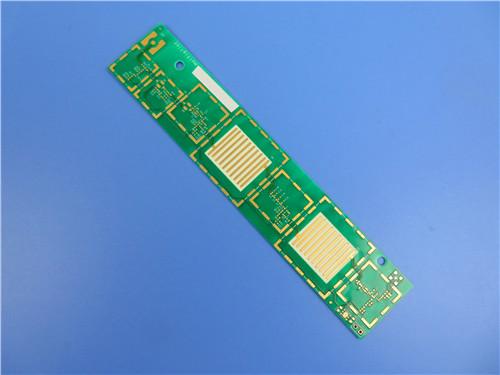
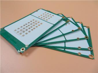
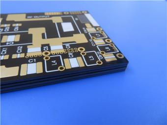
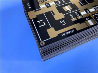
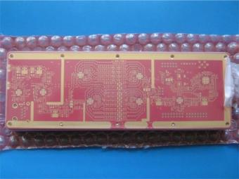
8-Layer RO4350B Tg180 FR-4Mixed Dielectric Material PCB Blind Buried Via ENIG
Product Overview
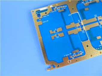
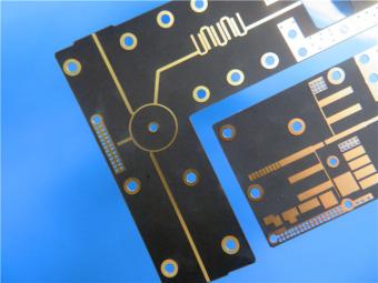
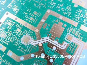
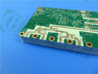
This 8-layer hybrid printed circuit board (PCB) is engineered for high-performance radio frequency (RF), microwave, and millimeter-wave applications that demand exceptional electrical stability, low signal loss, and reliable mechanical integrity. By combining Rogers RO4350B high-frequency ceramic-filled hydrocarbon laminates withhigh-Tg FR-4 core materials, this hybrid PCB achieves an optimal balance of premium RF performance, structural rigidity, and cost efficiency—making it ideal for aerospace, automotive radar, base station antennas, satellite communications, and high-speed data transmission systems.
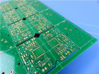
Built to IPC Class 3 standards, the board undergoes rigorous manufacturing and testing protocols to ensure consistent performance in mission-critical environments. With a compact form factor of 120 mmx 30 mm, it supports dense component integration while maintaining precise impedance control and minimal insertion loss across high-frequency bands. The 8-layer hybrid stackup leverages Rogers 4350B’s ultra-stable dielectric properties on outer layers for signal routing and high-Tg FR-4 inner layers for power distribution, ground planes, and structural support, creating a versatile platform for complex multi-functional electronic systems.

PCB Construction Details
This table summarizes the core mechanical, electrical, and structural specifications that define thehybrid circuitboard’s physical build and performance requirements.
|
Item |
Specification |
|
Base Material |
RO4350B+ Tg180 FR-4 |
|
Layer Count |
8 layers |
|
Board Dimensions |
120 mm × 30 mm (1 piece per panel) |
|
Finished Board Thickness |
1.553 mm |
|
Copper Weight |
Inner layers: 1 oz (1.4 mils); Outer layers: 1 oz (1.4 mils) |
|
Via Plating Thickness |
25 μm |
|
Blind Vias |
L1–L2 |
|
Buried Vias |
L5–L6 |
|
Surface Finish |
ENIG (Electroless Nickel Immersion Gold) |
|
Top Silkscreen |
White |
|
Bottom Silkscreen |
White |
|
Top Solder Mask |
Green |
|
Bottom Solder Mask |
Green |
|
Special Features |
Metal edge plating, resin plugged vias |
|
Quality Standard |
IPC Class 3 |
|
Pre-Shipment Test |
100% electrical performance test |
PCB Stackup
This table defines the layer sequence, material type, thickness, and copper distribution for the 8-layer PCB hybrid stackup.

Key Performance Advantages
1. Superior High-Frequency Electrical Performance
The outer layers utilize Rogers RO4350B, a leading high-frequency laminate with a stable dielectric constant (Dk = 3.66) and ultra-low dissipation factor (Df = 0.0031 at 10 GHz). This minimizes signal attenuation, phase shift, and insertion loss—critical for maintaining signal purity in 5G, radar, and satellite communication systems operating at 500 MHz to 40 GHz. Unlike standard FR-4,RO4350BPCB exhibits negligible Dk drift across temperature and frequency, ensuring consistent impedance control and repeatable circuit performance in extreme operating conditions.
2. Hybrid Material Optimization
The integration of Tg170 FR-4 core layers delivers exceptional mechanical strength, thermal stability, and cost effectiveness. With a glass transition temperature (Tg) of 170°C, the FR-4 core withstands lead-free soldering reflow temperatures without warping or delamination, while providing robust support for power distribution and internal signal routing. This hybrid approach eliminates the need for full-board high-frequency laminate usage, reducing material costs without compromising RF performance on critical outer layers.
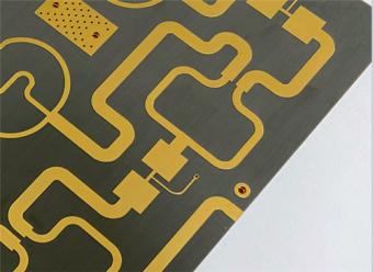
3. Advanced Via Technology for Signal Integrity
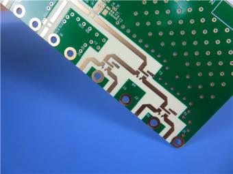
The board incorporates blind vias (1–2 layers) and buried vias (5–6 layers) to optimize routing density and signal integrity. Blind vias connect outer layers to adjacent inner layers without penetrating the entire board, reducing stub length and minimizing high-frequency signal reflection. Buried vias connect inner layers only, freeing up outer layer space for component placement and RF routing. Both via types are resin-plugged to prevent solder wicking and ensure planarization, while 25μm via plating guarantees reliable electrical conductivity and thermal dissipation.
4. IPC Class 3 Reliability
Built to IPC Class 3 standards—the highest for high-reliability electronic applications—thisHybrid PCB Board is designed for continuous operation in harsh environments where failure is not permissible. Every board undergoes 100% electrical testing before shipment to verify continuity, insulation resistance, and impedance compliance. Metal edge plating enhances structural rigidity, improves grounding performance, and protects board edges from mechanical damage and oxidation, extending service life in industrial and aerospace deployments.
Blind Vias & Buried Vias: Definition and Design Rationale
What Are Blind Vias?
Blind vias are plated through-holes that connect an outer layer to one or more inner layers but do not penetrate the entire board. In this design, blind vias connect Layer 1 (top RF layer) to Layer 2, allowing high-frequency signals to route downward without stubs that cause signal reflection and loss.
What Are Buried Vias?
Buried vias are plated through-holes located entirely within the inner layers of a multilayer PCB, connecting inner layers without reaching either outer layer. Here, buried vias connect Layer 5 to Layer 6, optimizing inner-layer routing and preserving outer-layer RF performance.
Why Use Blind and Buried Vias?
1)Improve RF Signal Integrity: Eliminate long via stubs that cause resonance, insertion loss, and impedance mismatch at high frequencies.
2)Increase Routing Density: Free up outer-layer space for RF traces and components by moving inner connections underground.
3)Reduce EMI: Shorten vertical signal paths and lower loop inductance to minimize electromagnetic radiation.
4)Enhance Thermal Performance: Improve heat dissipation from inner power layers to outer ground planes.
5)Meet Miniaturization Demands: Enable smaller form factors without sacrificing layer count or functionality.
RO4350B Ceramic-Filled Hydrocarbon Laminate (CCL) Technical Overview
Introduction to RO4350B
RO4350B is a high-performance, RoHS-compliant, flame-retardant (UL 94 V-0) ceramic-filled hydrocarbon laminate from Rogers Corporation, designed specifically for high-frequency RF and microwave circuits. It offers stable dielectric constant (Dk), low dissipation factor (Df), excellent thermal stability, and compatibility with standard FR-4 fabrication processes—no special etching or via preparation required (unlike PTFE materials). It is a drop-in upgrade for RO4003C and is widely used in cellular base stations, automotive radar, satellite LNBs, and broadband systems.
Key Advantages
RO4350B Technical Data Sheet
This table lists all critical mechanical, electrical, and thermal properties of RO4350B, tested per IPC and ASTM standards.
|
Property |
Typical Value (RO4350B) |
Direction |
Conditions |
Test Method |
|
Dielectric Constant, εᵣ (process) |
3.48 ± 0.05 |
Z |
10 GHz, 23 °C |
IPC TM 650 2.5.5.5 (Clamped Stripline) |
|
Dielectric Constant, εᵣ (design) |
3.66 |
Z |
8–40 GHz |
Differential Phase Length Method |
|
Dissipation Factor, tan δ |
0.0037 |
Z |
10 GHz, 23 °C |
IPC TM 650 2.5.5.5 |
|
Dissipation Factor, tan δ |
0.0031 |
Z |
2.5 GHz, 23 °C |
IPC TM 650 2.5.5.5 |
|
Thermal Coefficient of εᵣ |
+50 ppm/°C |
Z |
–50 °C to 150 °C |
IPC TM 650 2.5.5.5 |
|
Volume Resistivity |
1.2 × 10¹⁰ MΩ·cm |
– |
COND A |
IPC TM 650 2.5.17.1 |
|
Surface Resistivity |
5.7 × 10⁹ MΩ |
– |
COND A |
IPC TM 650 2.5.17.1 |
|
Electrical Strength |
31.2 KV/mm (780 V/mil) |
Z |
0.51 mm thickness |
IPC TM 650 2.5.6.2 |
|
Tensile Modulus |
16,767 MPa (X), 14,153 MPa (Y) |
X, Y |
RT |
ASTM D638 |
|
Tensile Strength |
203 MPa (X), 130 MPa (Y) |
X, Y |
RT |
ASTM D638 |
|
Flexural Strength |
255 MPa (37 kpsi) |
– |
– |
IPC TM 650 2.4.4 |
|
Dimensional Stability |
<0.5 mm/m (<0.5 mil/inch) |
X, Y |
After etch + E2/150°C |
IPC TM 650 2.4.39A |
|
CTE (Coefficient of Thermal Expansion) |
X: 10 ppm/°C, Y: 12 ppm/°C, Z: 32 ppm/°C |
X, Y, Z |
–55 °C to 288 °C |
IPC TM 650 2.4.41 |
|
Glass Transition Temperature (Tg) |
>280 °C (536 °F) |
– |
TMA method |
IPC TM 650 2.4.24.3 |
|
Decomposition Temperature (Td) |
390 °C (734 °F) |
– |
5% weight loss |
ASTM D3850 |
|
Thermal Conductivity |
0.69 W/m·K |
– |
80 °C |
ASTM C518 |
|
Moisture Absorption |
0.06% |
– |
48 hrs immersion, 50 °C |
ASTM D570 |
|
Density |
1.86 g/cm³ |
– |
23 °C |
ASTM D792 |
|
Copper Peel Strength |
0.88 N/mm (5.0 pli) |
– |
After solder float, 1 oz EDC foil |
IPC TM 650 2.4.8 |
|
Flammability |
(3) V 0 |
– |
– |
UL 94 |
|
Lead Free Process Compatible |
Yes |
– |
– |
– |
Standard Specifications
Typical Applications
Processing Guidelines for RO4350B
1)Storage: Store at 10–32°C (50–90°F), use FIFO inventory management.
2)Drilling: Surface speed 300–500 SFM; avoid >500 SFM. Use standard carbide drills.
3)Desmear: Typically not required for double-sided boards; multilayer boards may use alkaline permanganate or plasma desmear.
4)Plating: Compatible with standard electroless and electrolytic copper plating; 25μm via plating recommended.
5)Lamination: Compatible with most thermoset prepreg systems; follow prepreg bond profile.
6)Routing: Use carbide router bits, surface speed <500 SFM, chip load 0.0010–0.0015”/rev.
7)Surface Finish: Compatible with ENIG, HASL, OSP, and other standard finishes.
CCL Image Note
RO4350B appears as a rigid, light-colored ceramic-filled laminate with smooth copper cladding, available in ultrathin to standard core thicknesses. It is visually distinguishable from standard FR-4 by its higher density and uniform ceramic-loaded dielectric structure.

Conclusion
The 8-Layer RO4350B + Tg180 FR-4 hybrid PCB combines the best of two worlds: the superior high-frequency performance of RO4350B (low loss, stable Dk, FR-4 compatible processing) and the cost-effectiveness of FR-4 for non-critical layers. The inclusion of blind vias (1-2) and buried vias (5-6) significantly enhances signal integrity and routing density, while IPC Class 3 construction guarantees reliability in harsh environments. Metal edge plating and resin plugged vias add professional-grade shielding and assembly robustness. Supported by the exhaustive RO4350B laminate datasheet and processing knowledge provided above, this product stands as a ready-to-manufacture solution for next-generation RF and high-speed digital systems.


Previous:
4-Layer Rogers RO3003+TG170 FR-4 Hybrid PCB Immersion Silver Green Solder MaskNext:
4-layer RT/duroid 5880+TG175 FR4 Hybrid PCB with ENIG Controlled Depth SlotsIf you have questions or suggestions,please leave us a message,we will reply you as soon as we can!
Categories
New Products
Wangling 5mil 0.127mm TFA300 Core 2-layer Immersion Gold Green Solder Mask PCB
7.5mil AGC Taconic TLY-5 Substrate Custom PCB EPIG Finish Bare Copper
10mil Rogers CuClad 250 Immersion Gold 2-Layer Rigid Microwave PCB
20mil F4BTMS450 Wangling DK4.5 Laminate Custom PCB HASL LF Finsh
F4BME275 Wangling DK2.75 Laminate 2-Layer 1.6mm Pure Gold RF Custom PCB
Wangling F4BTD350S High Frequency PCB 2-layer 20mil Thick ENIG DK3.5 Substrate
12-layer TG200 TU-872 SLK High-Speed FR4 1.68mm PCB with ENIG Impedance Control
12-Layer RO4350B + RO3010 3.14mm Hybrid PCB Nickel-Free EPIG Surface Finish Blind Via
RO4003C exhibit a stable dielectric constant over a broad frequency range. This makes it an ideal substrate for broadband applications. And signal integrity performance improvement over the stack-ups with all FR4 board.
The hybrid PCB can be a mixture of FR-4 and high frequency material, and a mixture of high frequency material with different dielectric constant (DK)
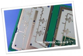
The 12mil core is on the top layer and it mainly plays the roles of signal layer. The core has fixed thickness which is very important to the electrical length of RF lines on the circuit board.
The hybrid PCB can be a mixture of FR-4 and high frequency material as abovementioned.
It contains 2 different boards in the panel. PCB boards are manufactured strictly as per required specifications with the standard IPC-Class-II.
Hybrid PCB is also known as mixed material lamination, it’s normally combined by two different material like FR4 and PI(rigid flex PCB), FR4 and Ceramic, FR4 and Teflon, FR4 and Aluminum base etc.
Hybrid constructions PCB typically involve a low loss material such as Nelco or Rogers combined with another core material like FR-4.
The Hybrid PCB on RO3003 and High Tg FR-4 is a state-of-the-art solution for high-frequency applications. With its exceptional stability, reliability, and manufacturability, it caters to the demands of industries such as automotive, telecommunications, and satellite communications.
 6-11C Shidai Jingyuan, Fuyong, Baoan, Shenzhen, Guangdong, China 518103


For inquiries about our products or pricelist, please leave to us and we will be in touch within 24 hours.
© Copyright: 2026 Shenzhen Bicheng Electronics Technology Co., Ltd.. All Rights Reserved.

IPv6 network supported


