

 Call Us Now !
Tel : +86 755 27374946
Call Us Now !
Tel : +86 755 27374946
 Order Online Now !
Email : info@bichengpcb.com
Order Online Now !
Email : info@bichengpcb.com
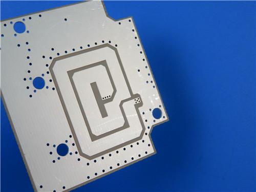
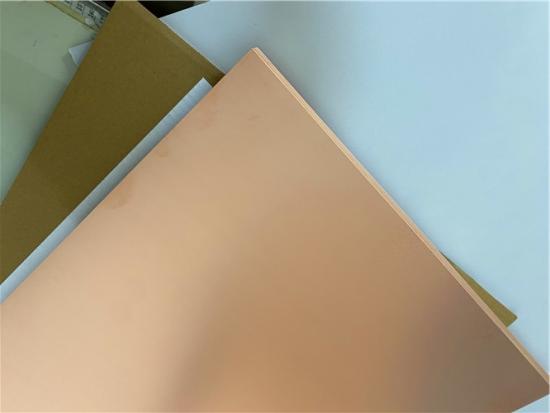
The TF960 PCB represents a carefully engineered balance of high-frequency electrical performance, thermal reliability, and manufacturing practicality.
Item NO.:
BIC-615-v700Order(MOQ):
1-10Payment:
T/TProduct Origin:
ChinaShipping Port:
ShenzhenLead Time:
7-10 days
Wangling TF960 Custom PCB High DK 9.6 Laminate 0.635mm Immersion Silver Finish
High-Frequency RF / Microwave Printed Circuit Board — Technical Product Description
Thisarticle presents a comprehensive technical overview of the TF960 PCB, a 2-layer rigid high-frequency printed circuit board built on a 0.635 mm TF960 ceramic-filled PTFE core with an immersion silver surface finish. Engineered for RF and microwave applications requiring ultra-low signal loss and precise impedance control, this board combines a dielectric constant (DK) of 9.6 at 10 GHz with a dissipation factor (Df) of just 0.0012, making it suitable for 5G/6G antenna systems, automotive and aerospace radar, satellite communications, and high-power RF amplifiers.
The following sections detail the PCB construction, layer stackup, manufacturing statistics, key performance features, and quality assurance. The description also concludes with an in-depth technical profile of the TF960 copper-clad laminate (CCL) material, providing engineers with a complete understanding of both the finished board and the substrate that underpins its performance.
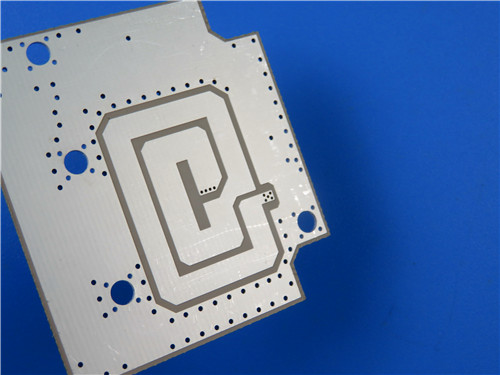
The Wangling TF960 PCB is a 2-layer rigid high-frequency circuit board measuring 102 mm × 86 mm per panel, with a finished board thickness of 0.7 mm. At its core lies a 0.635 mm (25 mil) TF960 laminate — a modified PTFE resin system reinforced with micron-sized ceramic fillers — clad with 35 μm (1 oz) copper on both outer layers. The board features an immersion silver surface finish, a blue solder mask on the top side, and white silkscreen for component identification.
The table below summarizes the key manufacturing and construction parameters of the 2-layer TF960 PCB, covering dimensional tolerances, feature capabilities, surface finishes, and quality assurance measures.
|
Parameter |
Specification |
|
Board Dimensions |
102 mm × 86 mm (1 PCS), ±0.15 mm |
|
Finished Board Thickness |
0.7 mm |
|
Minimum Trace / Space |
5 / 8 mils |
|
Minimum Hole Size |
0.25 mm |
|
Finished Copper Weight |
1 oz (35 μm / 1.4 mils) outer layers |
|
Via Plating Thickness |
20 μm |
|
Surface Finish |
Immersion Silver |
|
Top Solder Mask |
Blue |
|
Bottom Solder Mask |
None |
|
Top Silkscreen |
White |
|
Bottom Silkscreen |
None |
|
Blind / Buried Vias |
None |
|
Electrical Test |
100% tested prior to shipment |
|
Acceptance Standard |
IPC-Class-2 |
|
Artwork Format |
Gerber RS-274-X |
The board employs a symmetric 2-layer stackup with a TF960 dielectric cores and wiched between two 35 μm copper layers, as detailed in the table below. This simple, balanced structure ensures consistent impedance and minimizes warpage during assembly.
|
Layer |
Material |
Thickness |
|
Layer 1 (Top) |
Copper |
35 μm (1 oz) |
|
Core |
TF960 Dielectric |
0.635 mm (25 mils) |
|
Layer 2 (Bottom) |
Copper |
35 μm (1 oz) |
The following table provides a quantitative breakdown of the board's component and interconnect density, including pad counts, via quantities, and net count. These figures reflect the actual design data supplied in Gerber RS-274-X format.
|
Metric |
Count |
|
Total Components |
49 |
|
Total Pads |
57 |
|
Through-Hole Pads |
32 |
|
Top SMT Pads |
25 |
|
Bottom SMT Pads |
0 |
|
Vias |
43 |
|
Nets |
2 |
The TF960 Immersion Silver PCB delivers several differentiated performance characteristics that set it apart from conventional FR-4-based boards. First and foremost, the TF960 core offers a tightly controlled dielectric constant of 9.6 ± 0.19 at 10 GHz, enabling precise impedance matching in high-frequency circuits where even minor DK variations can degrade antenna gain and filter response. The ultra-low dissipation factor of 0.0012 at 10 GHz minimizes insertion loss, ensuring that signal power is efficiently transmitted through transmission lines rather than dissipated as heat in the dielectric.
Thermally, the material exhibits a coefficient of thermal expansion (CTE) of 50 ppm/℃ in both the X and Y axes and 65 ppm/℃ in the Z axis, providing excellent dimensional stability during reflow soldering and across operating temperature cycles. The Z-axis CTE of 65 ppm/℃ is notably lower than typical FR-4 values (70–90 ppm/℃), reducing the risk of plated-through-hole fatigue under thermal cycling. Furthermore, the board supports 260 ℃ lead-free assembly temperatures and carries a UL 94-V0 flammability rating, meeting modern regulatory and safety requirements.
Moisture absorption is rated at ≤ 0.05 %, significantly lower than standard FR-4 (typically 0.15–0.30 %), which ensures that dielectric properties remain stable in humid environments — a critical factor for outdoor RF equipment and aerospace applications. The high DK of 9.6 is particularly advantageous for miniaturizing antenna and filter designs, as higher dielectric constants allow for shorter guided-wavelength dimensions and more compact circuit layouts.
The immersion silver (ImAg) surface finish provides a flat, highly solderable surface with excellent contact resistance and signal integrity at high frequencies. Unlike HASL (Hot Air Solder Leveling), immersion silver offers a truly coplanar surface ideal for fine-pitch SMT components and high-frequency RF connectors. It is lead-free and RoHS-compliant, maintaining good shelf life when properly stored under dry conditions. The silver layer also provides low contact resistance, making it suitable for RF switch contacts, high-speed digital interfaces, and applications where repeated mating cycles are required.
The TF960 high frequency PCB is well-suited for a broad range of high-frequency applications, including:
• Microwave and RF transceivers for communication systems
• 5G / 6G massive MIMO antenna arrays and base station RF front-ends
• Automotive ADAS radar (77 GHz) and aerospace radar systems
• Satellite communication payloads and ground station equipment
• High-power RF amplifiers and power combiners / dividers
• Test and measurement equipment, including vector network analyzers
The TF960 PCB represents a carefully engineered balance of high-frequency electrical performance, thermal reliability, and manufacturing practicality. Its 0.635 mm TF960 core with DK 9.6 and Df 0.0012 at 10 GHz, combined with a robust 2-layer construction, immersion silver finish, and IPC-Class-2 quality assurance, makes it a dependable choice for RF and microwave designers seeking low-loss, dimensionally stable circuit boards.
The straightforward stackup and absence of blind vias also contribute to cost-effective fabrication without compromising high-frequency performance. The following section provides a detailed technical profile of the TF960 copper-clad laminate material itself, offering engineers deeper insight into the material properties that underpin this board's performance.
Part 2: CCL Material Knowledge — TF960 High-Frequency Laminate
TF960 is a high-frequency copper-clad laminate (CCL) belonging to the TF series of PTFE-ceramic composite dielectric substrates. The material is composed of polytetrafluoroethylene (PTFE) resin — renowned for its exceptional microwave performance and thermal stability — composited with micron-sized ceramic fillers. Unlike traditional FR-4 or even glass-reinforced PTFE laminates, the TFlaminateseries contains no glass fabric, relying instead on the ceramic filler to provide mechanical rigidity and to precisely tune the dielectric constant. By adjusting the ratio of ceramic filler to PTFE resin, manufacturers can achieve dielectric constants ranging from 3.0 to 16.0 across the TF product family, with TF960 specifically formulated to a DK of 9.6.
The TF naming convention distinguishes three product forms: TF denotes the bare dielectric material without copper cladding; TF-1 refers to single-sided copper-clad laminate; and TF-2 denotes double-sided copper-clad laminate, which is the form used in the TF960 PCB described in Part 1. This nomenclature system allows customers to select the appropriate cladding configuration based on their specific circuit design requirements.
TF960 offers a compelling set of material properties for high-frequency circuit designers:
• Dielectric constant of 9.6 at 10 GHz with a tight tolerance of ±0.19 (±2 %), ensuring consistent impedance control across production lots.
• Ultra-low dissipation factor of 0.0012 at 10 GHz, minimizing dielectric loss in microwave and millimeter-wave circuits.
• Long-term operating temperature range of -80 ℃ to +200 ℃, extending beyond the capabilities of conventional thermoplastic substrates.
• Available thickness range from 0.635 mm to 2.5 mm, accommodating a variety of impedance and mechanical requirements.
• Radiation resistance and low outgassing characteristics, making the material suitable for aerospace and space-borne applications.
• PCB processing compatibility with standard thermoplastic material fabrication workflows, including drilling, plating, and lamination.
The table below presents the complete technical specifications for TF960, including electrical, mechanical, thermal, and environmental properties, along with their respective test conditions and units. All values are typical measured data intended to assist customers in material selection.
|
Property |
Test Condition |
Unit |
TF960 Value |
|
Dielectric Constant (DK) |
10 GHz |
— |
9.6 ± 0.19 |
|
DK Tolerance |
— |
— |
±2 % |
|
Dissipation Factor (Df) |
10 GHz |
— |
0.0012 |
|
DK Temperature Coefficient |
-55 ℃ ~ 150 ℃ |
ppm/℃ |
-260 |
|
Peel Strength (1 oz, normal) |
Room temp |
N/mm |
> 0.6 |
|
Peel Strength (1 oz, after humidity) |
Damp-heat cycling |
N/mm |
> 0.4 |
|
Volume Resistivity |
500 V DC, normal |
MΩ·cm |
> 1 × 10⁹ |
|
Surface Resistance |
500 V DC, normal |
MΩ |
> 1 × 10⁷ |
|
CTE (X / Y / Z) |
-55 ℃ ~ 150 ℃ |
ppm/℃ |
50 / 50 / 65 |
|
Moisture Absorption |
20 ± 2 ℃, 24 h |
% |
≤ 0.05 |
|
Long-Term Operating Temperature |
Thermal chamber |
℃ |
-80 ~ 200 |
|
Material Composition |
— |
— |
PTFE + Ceramic + ED Copper Foil |
In addition to the electrical and mechanical parameters above, TF960 exhibits the following physical properties relevant to thermal management and weight-sensitive designs. The density of 3.02 g/cm³ reflects the high ceramic filler loading required to achieve the DK of 9.6, while the thermal conductivity of 0.68 W/(m·K) provides moderate heat-spreading capability for high-power RF circuits.
|
Property |
Unit |
Value |
|
Density |
g/cm³ |
3.02 |
|
Thermal Conductivity |
W/(m·K) |
0.68 |
TF960 laminate is offered in standard panel sizes and thicknesses, with ED (electrodeposited) copper foil cladding. The standard available panel sizes are 150 mm × 150 mm and 250 mm × 250 mm. Copper foil thickness options include 0.018 mm (1/2 oz) and 0.035 mm (1 oz). The table below lists the standard available dielectric thicknesses and their respective tolerances. Customers should specify whether the quoted thickness refers to the total copper-inclusive thickness or the dielectric-only thickness when placing orders. Non-standard thicknesses are available upon request.
|
Thickness (mm) |
Tolerance (mm) |
|
0.635 |
±0.04 |
|
0.8 |
±0.05 |
|
1.0 |
±0.05 |
|
1.2 |
±0.05 |
|
1.5 |
±0.06 |
|
2.0 |
±0.08 |
|
2.5 |
±0.10 |
TF960 is composed of PTFE resin, ceramic fillers, and ED copper foil. The absence of glass fabric in the TF series distinguishes it from glass-reinforced PTFE laminates and contributes to its isotropic dielectric properties — the DK measured in the Z-axis (thickness direction) is consistent and well-characterized, without the local variations that can occur near glass fiber bundles. The material is processed using standard PCB fabrication techniques compatible with thermoplastic materials, including mechanical drilling, electroless copper deposition, pattern plating, and solder mask application.
The peel strength of > 0.6 N/mm (1 oz copper, normal condition) and > 0.4 N/mm (after humidity cycling) ensures reliable copper-to-dielectric adhesion under typical operating conditions. The DK temperature coefficient of -260 ppm/℃ over the range of -55 ℃ to 150 ℃ indicates a slight decrease in DK with increasing temperature, which designers should account for in wide-temperature-range impedance simulations. The volume resistivity of > 1 × 10⁹ MΩ·cm and surface resistance of > 1 × 10⁷ MΩ confirm excellent insulating properties for high-voltage RF applications.
All TF960 material properties are characterized using recognized industry test methods. The dielectric constant is measured in the Z-axis direction using the stripline method per GB/T 12636-1990 or IPC-TM-650 2.5.5.5. Other electrical, mechanical, and thermal properties are tested in accordance with or by reference to IPC-TM-650 or GB/T 4722-2017 standards. All published data represent typical measured values intended to assist customers in material selection; they do not constitute an express or implied warranty, and customers are responsible for verifying the suitability of TF960 for their specific application requirements.
The image below shows the TF960 high-frequency copper-clad laminate material.
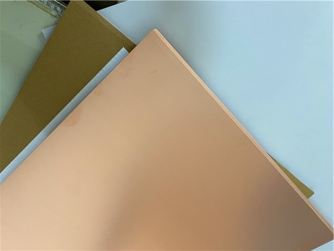
Figure 1: TF960 High-Frequency Copper-Clad Laminate
TF960 is a specialized high-frequency copper-clad laminate that combines the inherently low-loss characteristics of PTFE with the tunable dielectric properties of ceramic fillers, delivering a DK of 9.6 with exceptional stability and an ultra-low Df of 0.0012 at 10 GHz. Its broad operating temperature range (-80 ℃ to 200 ℃), low moisture absorption (≤ 0.05 %), radiation resistance, and low outgassing make it suitable for demanding applications spanning 5G/6G communications, automotive radar, aerospace, and satellite systems.
The glass-fabric-free construction ensures isotropic dielectric behavior and consistent Z-axis DK, while the standard thickness range of 0.635 mm to 2.5 mm and ED copper foil options of 1/2 oz and 1 oz provide designers with a flexible, well-characterized material platform. When fabricated into a 2-layer PCB with immersion silver finish — as detailed in Part 1 — TF960 delivers a reliable, high-performance solution for RF and microwave circuit designers who demand low insertion loss, precise impedance control, and long-term thermal and environmental stability.
Previous:
2-Layer F4BM233 4.0mm Wangling Substrate High-Frequency Custom PCB with ENIG FinishNext:
Wangling 2-Layer F4BTMS300 PCB 0.127mm DK3.0 Laminate ENIG Surface FinishIf you have questions or suggestions,please leave us a message,we will reply you as soon as we can!
Categories
New Products
Wangling TP2200 PCB 0.8mm Substrate Immersion Gold 2-Layer High-Dk (Dk 22) RF Board
Rogers TMM10 PCB 5.08mm Core ENIG 2-Layer High-Dk Microwave Board
Taconic TLX-8 PCB 50mil ENIG 2-Layer High-Frequency RF Circuit Board
Wangling TF440 25mil DK4.4 Laminate Immersion Gold 2-Layer Copper-filling Vias PCB
RO4360G2 Rogers 12mil ENEPIG 2-Layer DK6.15 High Frequency Custom PCB
Wangling F4BTMS220 2-Layer DK2.2 PCB 10 mil Core with Immersion Gold
Wangling F4BTME350 10mil DK3.5 High Frequency Substrate PCB 2-Layer Immersion Gold
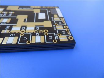
Wangling F4BTM300 Custom 2-layer PCB 20mil DK3.0 Substrate with Immersion Gold

RF-10 25mil Taconic PCB Materials stands out as a high-performance solution for RF applications. Its exceptional electrical properties, dimensional stability, thermal conductivity, and adhesion characteristics make it an ideal choice for demanding applications.
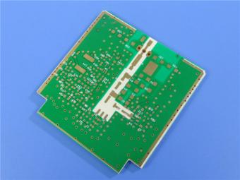
The PCB has a 4-layer hybrid stackup with a 0.5oz+plating ground layer, two 1oz ground layers, and a 0.5oz+plating signal layer.
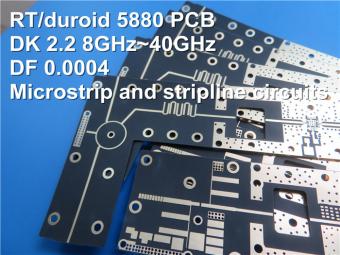
The dimensions of the board are 55.00 x 26.00 mm, with a tolerance of +/- 0.15mm. The board has 16 components, 26 total pads, 9 through-hole pads, 10 top SMT pads, 7 bottom SMT pads, 77 vias, and 82 nets.
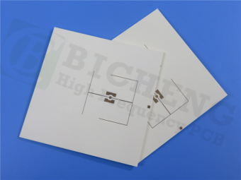
Rogers RO4003C PCB is an innovative and advanced circuit board that is made with high-quality materials.
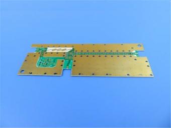
The RO4350B PCB offers a range of benefits that make it an ideal choice for high-frequency applications. Its low dielectric loss and high thermal conductivity make it perfect for high-frequency applications such as RF and microwave circuits.
Bicheng PCB Ships High-Quality PCBs with Shengyi Tg150 ℃ S1000H Material and Advanced Stackup
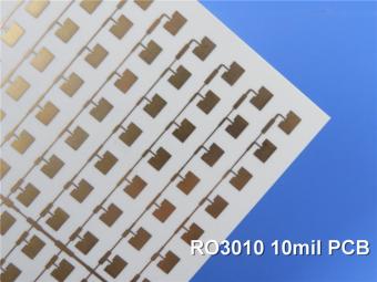
Rogers RO3010 PCB is ideal for a wide range of high-frequency applications, including power amplifiers, filters, couplers, and antennas.
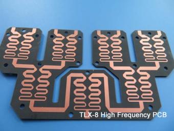
TLX-8 features low dielectric loss, low moisture absorption, and excellent thermal stability, making it ideal for high-frequency and high-speed applications. It has a low dissipation factor, which helps to minimize signal loss and distortion.
 6-11C Shidai Jingyuan, Fuyong, Baoan, Shenzhen, Guangdong, China 518103


For inquiries about our products or pricelist, please leave to us and we will be in touch within 24 hours.
© Copyright: 2026 Shenzhen Bicheng Electronics Technology Co., Ltd.. All Rights Reserved.

IPv6 network supported


