

 Call Us Now !
Tel : +86 755 27374946
Call Us Now !
Tel : +86 755 27374946
 Order Online Now !
Email : info@bichengpcb.com
Order Online Now !
Email : info@bichengpcb.com
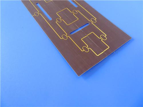
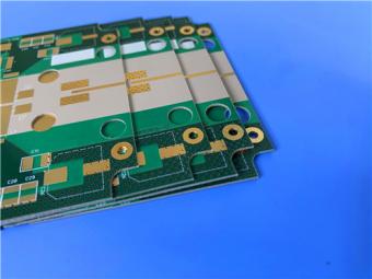
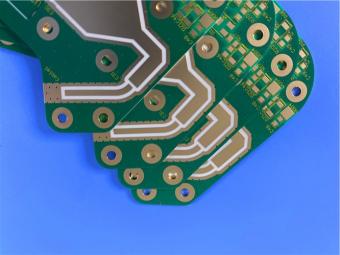
The 2-layer F4BTMS300 ENIG PCB with a 0.127 mm core represents a purpose-built solution for high-frequency applications demanding uncompromising signal integrity and thermal stability.
Item NO.:
BIC-613v698Order(MOQ):
1-10Payment:
T/TProduct Origin:
ChinaShipping Port:
ShenzhenLead Time:
7-10 days
Wangling 2-Layer F4BTMS300 PCB 0.127mm DK3.0 Laminate ENIG Surface Finish
This article provides a comprehensive technical description of a 2-layer rigid PCB fabricated on Wangling F4BTMS300, a PTFE-based ceramic-filled high-frequency laminate with a 0.127 mm dielectric core and ENIG (Electroless Nickel Immersion Gold) surface finish. The first part covers the PCB construction, layer stackup, design statistics, manufacturing quality, and target applications. The second part presents a detailed technical reference for the F4BTMS300 copper-clad laminate (CCL) material, including a complete data sheet, available configurations, and material characteristics.
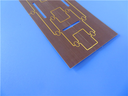
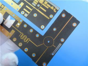
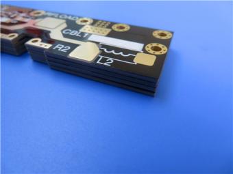
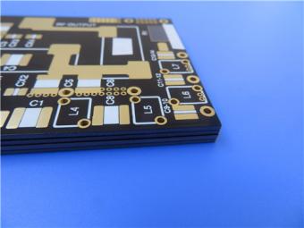
The 2-layer F4BTMS300 PCB is a high-frequency, high-reliability rigid circuit board engineered for microwave and RF applications where signal integrity and phase stability are critical. Built on a 0.127 mm (5 mil) F4BTMS300 core — a polytetrafluoroethylene (PTFE) laminate reinforced with ultra-thin, ultra-fine glass fiber cloth and loaded with uniformly dispersed nano-ceramic fillers — this board delivers a dielectric constant (Dk) of 3.00 at 10 GHz with a tight tolerance of ±0.04, and an ultra-low dissipation factor (Df) of 0.0013 at 10 GHz. The finished board thickness is 0.25 mm, with 1 oz (35 μm) copper on both outer layers and an ENIG surface finish for excellent solderability, flat coplanarity, and oxidation resistance.
Unlike conventional FR-4 boards, whose dielectric properties drift significantly at microwave frequencies and over temperature, the F4BTMS300 substrate maintains stable Dk and low loss across a frequency range up to 40 GHz and across an extreme temperature span from −55 °C to +150 °C, with a Dk temperature coefficient of just −20 ppm/°C. This stability makes the board particularly well suited for phase-sensitive antenna systems, phased-array radar, satellite communications, and aerospace equipment where consistent electrical performance under thermal cycling is non-negotiable. The material's low coefficient of thermal expansion (CTE) of 10/11/22 ppm/°C in the X/Y/Z directions — closely matched to copper's CTE of approximately 17 ppm/°C — further ensures the long-term reliability of plated through-holes under repeated thermal stress.
• Dielectric constant (Dk): 3.00 ± 0.04 at 10 GHz, enabling consistent impedance control in 50 Ω transmission lines.
• Dissipation factor (Df): 0.0013 at 10 GHz, 0.0015 at 20 GHz, and 0.0019 at 40 GHz — among the lowest in ceramic-filled PTFE laminates.
• Dk temperature coefficient: −20 ppm/°C from −55 °C to 150 °C, supporting phase-stable designs over wide temperature ranges.
• CTE: 10 / 11 / 22 ppm/°C (X / Y / Z) from −55 °C to 288 °C, closely matched to copper for reliable plated through-hole integrity.
• Thermal conductivity: 0.58 W/(m·K) in the Z direction, supporting moderate-power RF circuit layouts.
• Long-term operating temperature: −55 °C to +260 °C; UL-94 V-0 flammability rating.
• Moisture absorption: 0.025 % — exceptionally low, preserving RF performance in high-humidity environments.
The table below summarizes the physical dimensions, fabrication capabilities, surface finish, and quality-control specifications for this 2-layer PCB, providing a complete snapshot of its construction parameters.
|
Parameter |
Specification |
|
Board Dimensions |
66.04 mm × 78 mm (1 PCS), ±0.15 mm |
|
Minimum Trace / Space |
4 / 6 mils |
|
Minimum Hole Size |
0.35 mm |
|
Blind Vias |
None |
|
Finished Board Thickness |
0.25 mm |
|
Finished Copper Weight |
1 oz (1.4 mils / 35 μm), outer layers |
|
Via Plating Thickness |
20 μm |
|
Surface Finish |
ENIG (Electroless Nickel Immersion Gold) |
|
Top / Bottom Silkscreen |
None / None |
|
Top / Bottom Solder Mask |
None / None |
|
Electrical Test |
100 % tested prior to shipment |
|
Artwork Format |
Gerber RS-274-X |
|
Quality Standard |
IPC-Class-2 |
|
Availability |
Worldwide |
The board employs a symmetric 2-layer rigid stackup with equal 1 oz copper cladding on both sides of a single F4BTMS300 dielectric core, as detailed in the table below.
|
Layer |
Material |
Thickness |
|
Layer 1 (Top) |
Copper |
35 μm (1 oz) |
|
Core |
F4BTMS300 (PTFE + ceramic + glass fiber) |
0.127 mm (5 mil) |
|
Layer 2 (Bottom) |
Copper |
35 μm (1 oz) |
The design statistics below reflect the board's component count, pad configuration, via density, and net structure, offering a quick quantitative snapshot of the circuit's complexity.
|
Metric |
Count |
|
Components |
42 |
|
Total Pads |
38 |
|
Through-Hole Pads |
23 |
|
Top SMT Pads |
15 |
|
Bottom SMT Pads |
0 |
|
Vias |
26 |
|
Nets |
2 |
This PCB is manufactured using standard PTFE laminate processing techniques. TheF4BTMS300 material's excellent mechanical and physical properties make it well suited for fine-line and dense-hole fabrication. The demonstrated minimum trace/space of 4/6 mils and minimum drilled hole size of 0.35 mm confirm the board's manufacturability for moderately dense RF layouts without requiring specialized laser drilling or sequential lamination processes.
All boards undergo 100 % electrical testing prior to shipment, ensuring every circuit net meets continuity and isolation requirements. Production adheres to IPC-Class-2 quality standards — the most widely accepted class for commercial and industrial electronic products — and fabrication data is supplied in Gerber RS-274-X format, the industry standard for PCB manufacturing data interchange.
The ENIG surface finish provides a flat, coplanar surface ideal for fine-pitch SMT assembly and RF connector mounting. With a nickel layer underlying a thin gold coating, ENIG offers superior shelf life and solderability compared to HASL (Hot Air Solder Leveling), while avoiding the surface non-uniformity and coplanarity issues associated with solder leveling. The deliberate absence of solder mask and silkscreen on both layers is a common configuration in high-frequency RF boards: solder mask materials introduce localized dielectric discontinuities that can degrade signal performance at microwave frequencies, and bare boards are often housed in metal cavities or waveguide structures where silkscreen markings are unnecessary.
The combination of ultra-low loss, stable Dk over frequency and temperature, and aerospace-grade reliability makes thisWanglingPCB suitable for a broad range of high-frequency applications, including:
• Aerospace and avionics equipment, including space-borne and in-cabin electronics.
• Microwave and RF circuits, such as power amplifiers, low-noise amplifiers, and filters.
• Radar systems, including military radar and phased-array antenna feed networks.
• Phase-sensitive antennas and phased-array antenna systems.
• Satellite communications ground terminals and payload electronics.
• Test and measurement equipment operating at microwave frequencies.
The 2-layer F4BTMS300 ENIG PCB with a 0.127 mm core represents a purpose-built solution for high-frequency applications demanding uncompromising signal integrity and thermal stability. Its PTFE-ceramic composite substrate delivers a Dk of 3.00 with ±0.04 tolerance and a Df as low as 0.0013 at 10 GHz, while the symmetric 2-layer stackup with 1 oz copper and ENIG finish ensures reliable fabrication and assembly. With IPC-Class-2 quality assurance, 100 % electrical testing, and a material platform rated for −55 °C to +260 °C operation, this board is well positioned for aerospace, radar, satellite communication, and microwave RF systems where performance consistency across extreme environmental conditions is essential. The board's simple 2-layer architecture, combined with the exceptional high-frequency properties of F4BTMS300, offers a cost-effective yet high-performance platform for designers seeking FR-4 alternatives in the 1–40 GHz range.
The F4BTMS series is an upgraded generation of the F4BTM series of PTFE-based high-frequency copper-clad laminates. Through breakthroughs in material formulation and manufacturing processes, the F4BTMS series incorporates a high loading of ceramic fillers reinforced with ultra-thin, ultra-fine glass fiber cloth. This architecture delivers substantially improved material performance, a broader range of available dielectric constants, and aerospace-grade reliability that enables it to substitute for comparable imported products.
The key technological innovation lies in the material composition: a small quantity of ultra-thin, ultra-fine glass fiber cloth is combined with a large volume of uniformly dispersed special nano-ceramic particles mixed with polytetrafluoroethylene (PTFE) resin. This formulation minimizes the "glass fiber effect" — the localized dielectric non-uniformity caused by conventional woven glass cloth that can distort electromagnetic wave propagation at microwave frequencies. The result is reduced dielectric loss, enhanced dimensional stability, decreased X/Y/Z anisotropy, an extended usable frequency range, improved electrical strength, and higher thermal conductivity. The material also exhibits an excellent low coefficient of thermal expansion and stable dielectric temperature characteristics.
The F4BTMS series comes standard with RTF (Reverse Treated Foil) low-roughness copper foil, which reduces conductor loss — a critical factor at microwave frequencies where the skin depth is extremely small — while maintaining excellent peel strength (>1.2 N/mm for 1 oz copper). The series can be supplied with either copper or aluminum bases for applications requiring electromagnetic shielding or enhanced thermal dissipation.
• Tight dielectric constant tolerance (±0.04) with excellent batch-to-batch consistency.
• Ultra-low dissipation factor across the full operating frequency range up to 40 GHz.
• Stable Dk and low loss up to 40 GHz, satisfying phase-sensitive application requirements.
• Excellent Dk and Df temperature coefficients, maintaining frequency and phase stability from −55 °C to 150 °C.
• Outstanding radiation resistance — dielectric and physical properties remain stable after specified radiation dose exposure.
• Low outgassing performance, meeting aerospace vacuum outgassing requirements when tested per standard methods.
• Low CTE in X/Y/Z directions, ensuring dimensional thermal stability and plated through-hole reliability.
• Improved thermal conductivity for higher-power application scenarios.
• Excellent dimensional stability and low moisture absorption (0.025 %).
The following table presents the complete electrical, mechanical, thermal, and physical property data for the F4BTMS300 laminate. All values are typical measurements tested per IPC-TM-650 or GB/T 4722-2017 standard methods, and are intended to assist customers in material selection.
|
Property |
Test Condition |
Unit |
F4BTMS300 |
|
Dk (Typical) |
10 GHz |
— |
3.00 |
|
Dk Tolerance |
— |
— |
±0.04 |
|
Dk (Design Value) |
10 GHz |
— |
3.0 |
|
Df (Typical) |
10 GHz |
— |
0.0013 |
|
Df (Typical) |
20 GHz |
— |
0.0015 |
|
Df (Typical) |
40 GHz |
— |
0.0019 |
|
Dk Temp. Coefficient |
−55 °C ~ 150 °C |
ppm/°C |
−20 |
|
Peel Strength |
1 oz RTF Cu |
N/mm |
>1.2 |
|
Volume Resistivity |
Normal |
MΩ·cm |
≥1×10⁸ |
|
Surface Resistance |
Normal |
MΩ |
≥1×10⁸ |
|
Electrical Strength (Z) |
5 kW, 500 V/s |
kV/mm |
>40 |
|
Breakdown Voltage (XY) |
5 kW, 500 V/s |
kV |
>52 |
|
CTE (X, Y) |
−55 °C ~ 288 °C |
ppm/°C |
10, 11 |
|
CTE (Z) |
−55 °C ~ 288 °C |
ppm/°C |
22 |
|
Thermal Stress |
260 °C, 10 s, 3 cycles |
— |
No delamination |
|
Water Absorption |
20±2 °C, 24 h |
% |
0.025 |
|
Density |
Room temp. |
g/cm³ |
2.28 |
|
Long-Term Use Temp. |
High/low temp. chamber |
°C |
−55 ~ +260 |
|
Thermal Conductivity |
Z direction |
W/(m·K) |
0.58 |
|
Flammability |
— |
UL-94 |
V-0 |
|
Material Composition |
— |
— |
PTFE, ultra-fine glass fiber, ceramic |
Notes: (1) Dk typical value is measured in the Z direction using the stripline method per GB/T 12636-1990 or IPC-TM-650 2.5.5.5. (2) Other properties are tested per or in reference to IPC-TM-650 or GB/T 4722-2017. (3) All data are typical measurements intended to assist material selection and do not constitute an express or implied warranty. Customers are responsible for verifying the suitability of the material in each specific application.
The F4BTMS300 laminate can be supplied with the following copper foil configurations to meet diverse design requirements:
• Standard thickness:0.5 oz (0.018 mm) and 1 oz (0.035 mm); other thicknesses available by custom order.
• Standard foil type:RTF (Reverse Treated Foil) low-roughness copper foil, minimizing conductor loss at microwave frequencies.
• 50 Ω embedded resistor copper foil:The resistor film consists of a nickel-phosphorus (Ni-P) alloy with a thickness of 0.2 μm, providing a sheet resistance of 50 ± 5 Ω per square. This option enables the construction of resistor-embedded laminates, reducing the need for discrete surface-mount resistors in RF attenuator and termination circuits.
• Aluminum base (F4BTMS300-AL):Dielectric layer clad with copper foil on one side and aluminum on the other, providing electromagnetic shielding and enhanced thermal dissipation.
• Copper base (F4BTMS300-CU):Dielectric layer clad with copper foil on one side and a copper metal base on the other, for maximum thermal conductivity in high-power RF applications.
Standard panel sizes for F4BTMS300 laminate include the following; custom sizes are available upon request:
• 305 × 460 mm (12" × 18")
• 460 × 610 mm (18" × 24")
• 610 × 920 mm (24" × 36")
For F4BTMS300, the minimum dielectric thickness is 0.127 mm (5.0 mil), and the material is available in thicknesses that are multiples of 0.127 mm. The table below lists standard thickness options and their corresponding tolerances.
|
Thickness (mm / mil) |
Tolerance (mm / mil) |
|
0.127 / 5.0 |
±0.0127 / 0.5 |
|
0.254 / 10 |
±0.02 / 1.0 |
|
0.508 / 20 |
±0.03 / 1.19 |
|
0.635 / 25 |
±0.04 / 1.58 |
|
0.762 / 30 |
±0.04 / 1.58 |
|
1.016 / 40 |
±0.05 / 2.0 |
|
1.270 / 50 |
±0.05 / 2.0 |
|
1.524 / 60 |
±0.06 / 2.5 |
|
2.03 / 80 |
±0.08 / 3.2 |
|
2.54 / 100 |
±0.10 / 4.0 |
|
3.175 / 125 |
±0.13 / 5.0 |
|
4.06 / 160 |
±0.18 / 7.0 |
|
5.08 / 200 |
±0.20 / 8.0 |
|
6.35 / 250 |
±0.25 / 10 |
The F4BTMS series can be supplied with a metal base (aluminum or copper) bonded to one side of the dielectric, with copper foil on the opposite side. This configuration provides electromagnetic shielding and enhanced thermal dissipation for high-power RF circuits. The model naming convention is F4BTMS-AL for aluminum-base and F4BTMS-CU for copper-base laminates (e.g., F4BTMS300-AL, F4BTMS300-CU).
|
Model |
Metal Base |
Density (g/cm³) |
Thermal Cond. (W/m·K) |
CTE (ppm/°C) |
|
F4BTMS300-CU |
Purple copper / brass |
8.9 |
380 |
17 |
|
F4BTMS300-AL |
Aluminum |
2.7 |
180 |
24 |
For the copper-base variant (F4BTMS300-CU), available metal base thicknesses include 0.48, 0.98, 1.48, 1.98, 2.98, and 3.98 mm (other thicknesses available by custom order), with a thickness tolerance of +0.02 / −0.05 mm. Standard panel sizes for copper-base laminates are 460 × 610 mm and 460 × 305 mm.
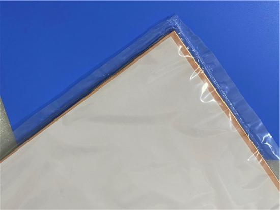
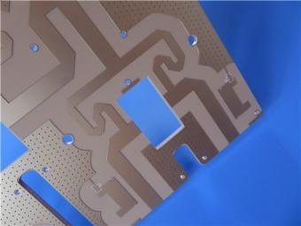
The image below shows the F4BTMS300 copper-clad laminate material, illustrating its physical appearance as a high-frequency PTFE-ceramic composite substrate.
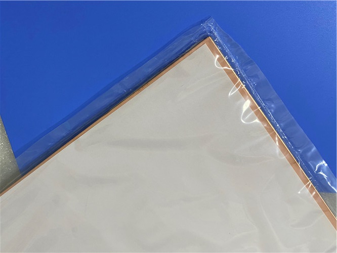
Figure 1: F4BTMS300 Copper-Clad Laminate
The F4BTMS300 copper-clad laminate is a high-performance, aerospace-grade PTFE-based material that combines ultra-low dielectric loss (Df = 0.0013 at 10 GHz), tight Dk tolerance (±0.04), and exceptional thermal and dimensional stability. Its unique nano-ceramic and ultra-fine glass fiber reinforcement minimizes the glass fiber effect, making it suitable for phase-sensitive microwave and millimeter-wave applications up to 40 GHz. With a long-term operating temperature range of −55 °C to +260 °C, UL-94 V-0 flammability, low outgassing for space environments, and versatile options including RTF copper foil, embedded resistor foil, and aluminum/copper metal bases, F4BTMS300 offers a comprehensive material platform for the most demanding high-frequency PCB designs. Its performance is comparable to leading international PTFE-ceramic laminates, providing a reliable alternative for aerospace, radar, satellite communication, and high-end RF applications where material consistency and long-term reliability are paramount.
Previous:
Wangling TF960 Custom PCB High DK 9.6 Laminate 0.635mm Immersion Silver FinishNext:
Wangling 2-Layer F4BME220 PCB 3.9 mil DK 2.2 Laminate Immersion Gold Surface FinishIf you have questions or suggestions,please leave us a message,we will reply you as soon as we can!
Categories
New Products
Wangling F4BTMS220 2-Layer DK2.2 PCB 10 mil Core with Immersion Gold
Wangling F4BTME350 10mil DK3.5 High Frequency Substrate PCB 2-Layer Immersion Gold
Wangling F4BTM300 Custom 2-layer PCB 20mil DK3.0 Substrate with Immersion Gold
Rogers 20mil RT/duroid 6202 2-layer ENIG High-Frequency Microwave PCB
Rogers 20mil AD250C PCB Pure Gold High-Frequency Antenna Circuit Board
8-Layer Hybrid RF PCB: RO4350B + TG170 FR-4 + RO4003C with RO4450F Bondply
4-Layer Rogers RO3010 Hybrid PCB Immersion Silver 2.8mm Finished Thickness
4-Layer 20mil Rogers RO3210 ISIG High-Frequency PCB with Controlled Depth Milling

RF-10 25mil Taconic PCB Materials stands out as a high-performance solution for RF applications. Its exceptional electrical properties, dimensional stability, thermal conductivity, and adhesion characteristics make it an ideal choice for demanding applications.
The PCB has a 4-layer hybrid stackup with a 0.5oz+plating ground layer, two 1oz ground layers, and a 0.5oz+plating signal layer.
The dimensions of the board are 55.00 x 26.00 mm, with a tolerance of +/- 0.15mm. The board has 16 components, 26 total pads, 9 through-hole pads, 10 top SMT pads, 7 bottom SMT pads, 77 vias, and 82 nets.
Rogers RO4003C PCB is an innovative and advanced circuit board that is made with high-quality materials.
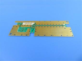
The RO4350B PCB offers a range of benefits that make it an ideal choice for high-frequency applications. Its low dielectric loss and high thermal conductivity make it perfect for high-frequency applications such as RF and microwave circuits.
Bicheng PCB Ships High-Quality PCBs with Shengyi Tg150 ℃ S1000H Material and Advanced Stackup
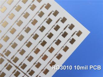
Rogers RO3010 PCB is ideal for a wide range of high-frequency applications, including power amplifiers, filters, couplers, and antennas.
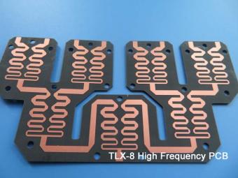
TLX-8 features low dielectric loss, low moisture absorption, and excellent thermal stability, making it ideal for high-frequency and high-speed applications. It has a low dissipation factor, which helps to minimize signal loss and distortion.
 6-11C Shidai Jingyuan, Fuyong, Baoan, Shenzhen, Guangdong, China 518103


For inquiries about our products or pricelist, please leave to us and we will be in touch within 24 hours.
© Copyright: 2026 Shenzhen Bicheng Electronics Technology Co., Ltd.. All Rights Reserved.

IPv6 network supported


