

 Call Us Now !
Tel : +86 755 27374946
Call Us Now !
Tel : +86 755 27374946
 Order Online Now !
Email : info@bichengpcb.com
Order Online Now !
Email : info@bichengpcb.com
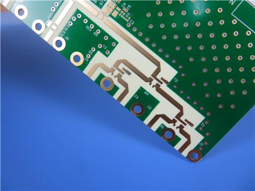
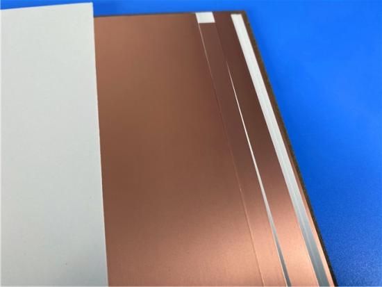
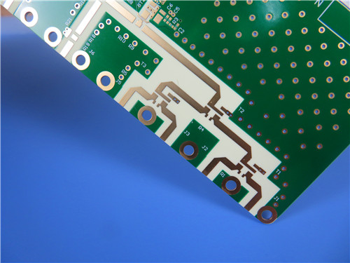
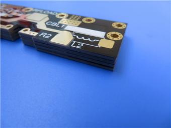
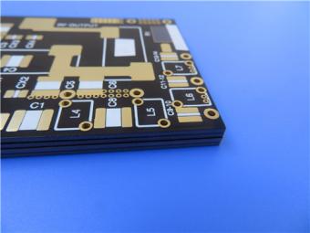
This 12-layer RO4350B+RO3010 hybrid PCB exemplifies the state-of-the-art in high-frequency circuit board design.
Item NO.:
BIC-590-v675.0Order(MOQ):
1-10Payment:
T/TProduct Origin:
ChinaShipping Port:
ShenzhenLead Time:
7-10 days
12-Layer RO4350B + RO3010 3.14mm Hybrid PCB Nickel-Free EPIG Surface Finish Blind Via
1. Product Overview & Core Differentiation
This 12-layer hybrid RF/microwave board integrates two proprietaryRogers high-frequency core materials—hydrocarbon ceramic RO4350B and ceramic-filled PTFE RO3010—bonded with RO4450F prepreg, paired with nickel-free EPIG (Electroless Palladium Immersion Gold) surface finish. It is engineered for mixed-signal wideband RF systems that simultaneously demand ultra-low high-frequency loss, high dielectric constant antenna layers, low-cost mass manufacturability, and multi-stage HDI blind via interconnection.
Unlike single-material RF PCBs that force tradeoffs between antenna gain, broadband signal stability and fabrication cost, this hybrid stackup partitions electrical functions by material characteristics: RO3010 handles high-Dk antenna resonant layers for compact patch antenna arrays, while RO4350B forms intermediate power/ground stripline layers with FR-4-compatible processing, eliminating the specialized sodium etch required for pure PTFE multilayer boards.
2. PCB Construction Details
The construction details below summarize the key manufacturing parameters that define thishybrid PCB's physical and electrical characteristics.
|
Parameter |
Specification |
|
Base Material |
RO4350B + RO3010 + RO4450F Prepreg |
|
Layer Count |
12 Layers |
|
Board Dimensions |
107mm x 91.5mm = 2PCS, +/- 0.15mm |
|
Finished Board Thickness |
3.14mm |
|
Finished Copper Weight (Outer Layers) |
1 oz (35μm) |
|
Finished Copper Weight (Inner Layers) |
0.5 oz (18μm) |
|
Surface Finish |
EPIG (Nickel-free) |
|
Top Silkscreen Color |
White |
|
Bottom Silkscreen Color |
White |
|
Top Solder Mask Color |
Green |
|
Bottom Solder Mask Color |
Green |
|
Electrical Testing |
100% Electrical Test Prior to Shipment |
|
Blind Via Structures |
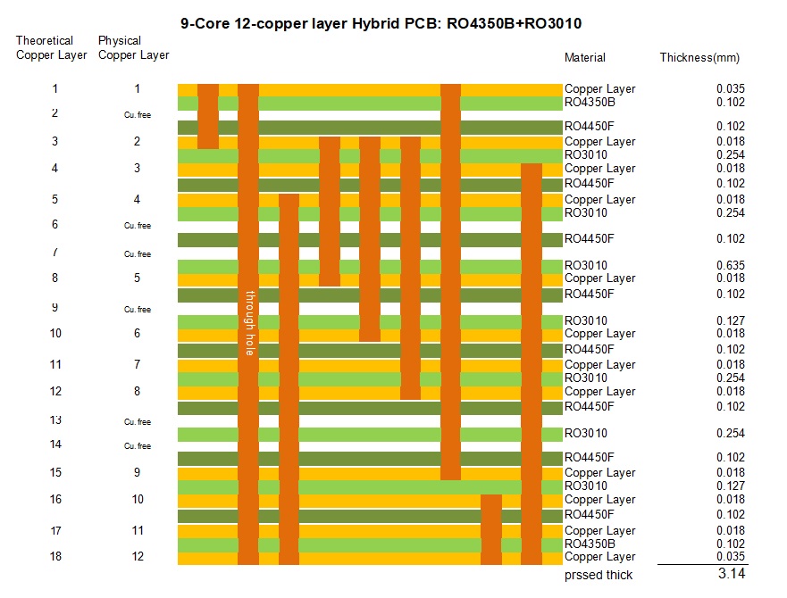
1-2, 2-5, 2-6, 2-8, 1-9, 10-12, 3-12 |
3. PCB Layer Stackup
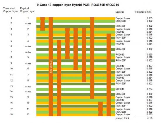
The following stackup table details the precise material arrangement and thickness distribution that enables this Hybrid PCB Board's hybrid performance characteristics.
4. Key Process & Performance Advantages of Hybrid Construction
4.1 Multi-Material Lamination Reliability
4.2 Nickel-Free EPIG Surface Finish RF Performance Breakthrough
4.3 Sequential Blind Via HDI Design Optimization
4.4 Electrical & Thermal Stability Under Wide Operating Temperatures
5. PCB Application Scenarios
This hybrid 12-layer EPIG PCB targets high-performance mixed RF/digital systems requiring both compact high-Dk antenna design and broadband low-loss signal processing:
6. PCB Conclusion
This 12-layer RO4350B+RO3010 hybrid PCB exemplifies the state-of-the-art in high-frequency circuit board design. The intelligent combination of three material systems—RO4350B for its low-loss, FR-4 compatible processing characteristics; RO3010 for its high dielectric constant enabling circuit miniaturization; and RO4450F for reliable multilayer lamination—creates a structure that achieves performance levels unattainable with single-material solutions. Thenickel-free EPIG finish, comprehensive blind via architecture, and precise thickness control of 3.14mm collectively deliver a platform suitable for demanding applications including 5G infrastructure, automotive radar, aerospace communications, and advanced test equipment.
The hybrid approach demonstrated here offers designers the flexibility to optimize individual layer properties while maintaining overall board integrity. The CTE-matched materials (RO4350B: 10-12 ppm/°C X/Y; RO3010: 13/11 ppm/°C X/Y) provide exceptional dimensional stability across temperature extremes, ensuring reliable performance in environmentally challenging conditions.
Supplementary CCL Laminate Technical Knowledge
Section Summary: Complete Datasheet Parameter Comparison of RO3010 and RO4350B Rogers High-Frequency Copper Clad Laminates, covering material composition, electrical, thermal, mechanical and manufacturability differences with standardized test data and structural characteristic explanation
1. Material Core Composition Classification
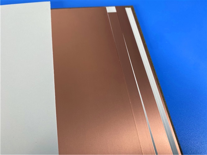
Two distinct Rogers CCL technology platforms form the hybrid PCB’s dielectric foundation, with fundamentally different resin matrix chemistries driving performance and processing divergence:
2. RO4350B & RO3010 Data Sheet
2.1 RO4350B Data Sheet
|
Property |
RO4350B |
Units |
Condition |
|
Dielectric Constant, εr (Process) |
3.48 ± 0.05 |
- |
10 GHz, 23°C |
|
Dielectric Constant, εr (Design) |
3.66 |
- |
8-40 GHz |
|
Dissipation Factor (tan δ) |
0.0037 / 0.0031 |
- |
10 GHz / 2.5 GHz, 23°C |
|
Thermal Coefficient of εr |
50 |
ppm/°C |
-50°C to 150°C |
|
Volume Resistivity |
1.2 × 10¹⁰ |
MΩ·cm |
COND A |
|
Surface Resistivity |
5.7 × 10⁹ |
MΩ |
COND A |
|
Electrical Strength |
31.2 (780) |
KV/mm (V/mil) |
0.51mm thickness |
|
Tensile Modulus (X/Y) |
16,767 / 14,153 |
MPa (ksi) |
RT, ASTM D638 |
|
Tensile Strength (X/Y) |
203 / 130 |
MPa (ksi) |
RT, ASTM D638 |
|
Flexural Strength |
255 (37) |
MPa (kpsi) |
IPC-TM-650 2.4.4 |
|
Dimensional Stability |
<0.5 |
mm/m (mils/inch) |
After etch +E2/150°C |
|
CTE (X/Y/Z) |
10/12/32 |
ppm/°C |
-55°C to 288°C |
|
Tg (TMA) |
>280 |
°C |
IPC-TM-650 2.4.24.3 |
|
Td (TGA) |
390 |
°C |
ASTM D3850 |
|
Thermal Conductivity |
0.69 |
W/m/°K |
80°C, ASTM C518 |
|
Moisture Absorption |
0.06 |
% |
48 hrs immersion, 50°C |
|
Density |
1.86 |
g/cm³ |
23°C, ASTM D792 |
|
Copper Peel Strength |
0.88 (5.0) |
N/mm (pli) |
After solder float, 1 oz EDC |
|
Flammability |
(3) V-0 |
- |
UL 94 |
|
Lead-Free Process Compatible |
Yes |
- |
- |
2.2 RO3010 Data Sheet
|
Property |
Typical Value |
Units |
Test Condition |
Test Method |
|
Dielectric Constant (Process) |
10.2 ± 0.30 |
– |
10 GHz / 23°C |
IPC-TM-650 2.5.5.5 |
|
Dielectric Constant (Design) |
11.2 |
– |
8 – 40 GHz |
Differential Phase Length |
|
Dissipation Factor |
0.0022 |
– |
10 GHz / 23°C |
IPC-TM-650 2.5.5.5 |
|
Thermal Coefficient of Dk |
-395 |
ppm/°C |
-50 to 150°C / 10 GHz |
IPC-TM-650 2.5.5.5 |
|
Volume Resistivity |
10⁵ |
MΩ·cm |
Condition A |
IPC-TM-650 2.5.17.1 |
|
Surface Resistivity |
10⁵ |
MΩ |
Condition A |
IPC-TM-650 2.5.17.1 |
|
Decomposition Temperature (Td) |
>500 |
°C (TGA) |
– |
ASTM D3850 |
|
CTE (X-axis) |
13 |
ppm/°C |
-55 to 288°C |
IPC-TM-650 2.4.41 |
|
CTE (Y-axis) |
11 |
ppm/°C |
-55 to 288°C |
IPC-TM-650 2.4.41 |
|
CTE (Z-axis) |
16 |
ppm/°C |
-55 to 288°C |
IPC-TM-650 2.4.41 |
|
Thermal Conductivity |
0.95 |
W/(m·K) |
50°C |
ASTM D5470 |
|
Copper Peel Strength |
9.4 |
lbs/in |
1 oz ED copper after solder float |
IPC-TM-650 2.4.8 |
|
Young’s Modulus |
1902 (MD), 1934 (CMD) |
MPa |
23°C |
ASTM D638 |
|
Dimensional Stability |
-0.35 (MD), -0.31 (CMD) |
mm/m |
Condition A |
IPC-TM-650 2.2.4 |
|
Flammability |
V-0 |
– |
UL 94 |
UL 94 |
|
Moisture Absorption |
0.05 |
% |
D48/50 |
IPC-TM-650 2.6.2.1 |
|
Density |
2.8 |
g/cm³ |
23°C |
ASTM D792 |
|
Specific Heat Capacity |
0.8 |
J/(g·K) |
– |
Calculated |
|
Lead Free Process Compatible |
Yes |
– |
– |
– |
3. Available Standard Configurations for RO3010 & RO4350B CCL
3.1 RO3010 Standard Specifications
3.2 RO4350B Standard Specifications
4. Material Application Partition Logic in Hybrid PCB Stackup
The physical property gaps between RO3010 and RO4350B dictate their layer assignment in the12-layer hybrid board, with clear functional separation to maximize system performance:
5. CCL Section Conclusion
Rogers RO3010 and RO4350B represent two complementary high-frequency CCL technology families with distinct electrical, thermal and manufacturing characteristics, each optimized for separate RF circuit functions. RO3010’s PTFE-ceramic construction delivers unrivaled millimeter-wave loss performance and high permittivity for compact antenna design, while RO4350B’s hydrocarbon thermoset platform balances low production cost, FR-4-compatible processing and stable broadband impedance for intermediate power and signal layers.
Their closely matched CTE profiles enable reliable hybrid lamination with RO4450F prepreg, eliminating the warpage and delamination risks common to mismatched multi-material PCB stacks. The intentional combination of these two laminates in the 12-layer hybrid EPIG PCB unlocks performance levels unachievable with a single substrate material, creating a cost-effective, high-reliability material solution for modern mixed-signal millimeter-wave wireless and automotive radar hardware.
Previous:
4-layer 5mil RT6202 + FR-4 Hybrid PCB 1.014mm ENIG Resin Plug ViasNext:
8-Layer Hybrid PCB RO4003C + S1000-2M FR4 with ENIG Surface Finish Blind ViaIf you have questions or suggestions,please leave us a message,we will reply you as soon as we can!
Categories
New Products
Wangling F4BTMS220 2-Layer DK2.2 PCB 10 mil Core with Immersion Gold
Wangling F4BTME350 10mil DK3.5 High Frequency Substrate PCB 2-Layer Immersion Gold
Wangling F4BTM300 Custom 2-layer PCB 20mil DK3.0 Substrate with Immersion Gold
Rogers 20mil RT/duroid 6202 2-layer ENIG High-Frequency Microwave PCB
Rogers 20mil AD250C PCB Pure Gold High-Frequency Antenna Circuit Board
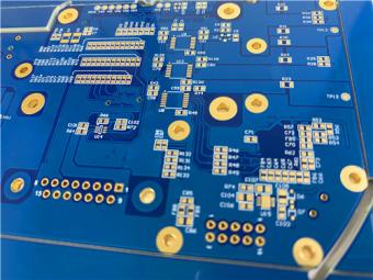
8-Layer Hybrid RF PCB: RO4350B + TG170 FR-4 + RO4003C with RO4450F Bondply
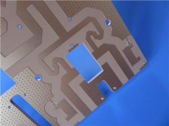
4-Layer Rogers RO3010 Hybrid PCB Immersion Silver 2.8mm Finished Thickness
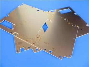
4-Layer 20mil Rogers RO3210 ISIG High-Frequency PCB with Controlled Depth Milling
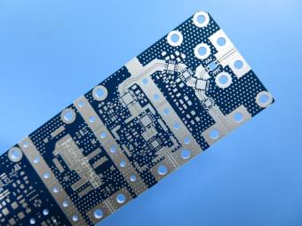
RO4003C exhibit a stable dielectric constant over a broad frequency range. This makes it an ideal substrate for broadband applications. And signal integrity performance improvement over the stack-ups with all FR4 board.
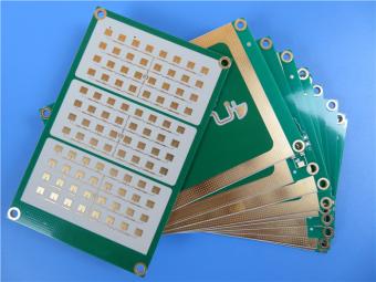
The hybrid PCB can be a mixture of FR-4 and high frequency material, and a mixture of high frequency material with different dielectric constant (DK)
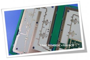
The 12mil core is on the top layer and it mainly plays the roles of signal layer. The core has fixed thickness which is very important to the electrical length of RF lines on the circuit board.
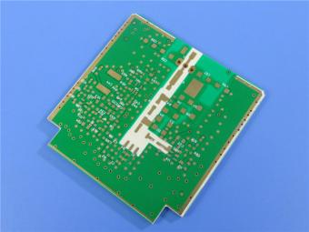
The hybrid PCB can be a mixture of FR-4 and high frequency material as abovementioned.
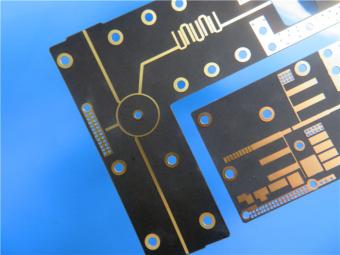
It contains 2 different boards in the panel. PCB boards are manufactured strictly as per required specifications with the standard IPC-Class-II.
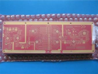
Hybrid PCB is also known as mixed material lamination, it’s normally combined by two different material like FR4 and PI(rigid flex PCB), FR4 and Ceramic, FR4 and Teflon, FR4 and Aluminum base etc.
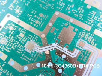
Hybrid constructions PCB typically involve a low loss material such as Nelco or Rogers combined with another core material like FR-4.
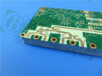
The Hybrid PCB on RO3003 and High Tg FR-4 is a state-of-the-art solution for high-frequency applications. With its exceptional stability, reliability, and manufacturability, it caters to the demands of industries such as automotive, telecommunications, and satellite communications.
 6-11C Shidai Jingyuan, Fuyong, Baoan, Shenzhen, Guangdong, China 518103


For inquiries about our products or pricelist, please leave to us and we will be in touch within 24 hours.
© Copyright: 2026 Shenzhen Bicheng Electronics Technology Co., Ltd.. All Rights Reserved.

IPv6 network supported


