

 Call Us Now !
Tel : +86 755 27374946
Call Us Now !
Tel : +86 755 27374946
 Order Online Now !
Email : info@bichengpcb.com
Order Online Now !
Email : info@bichengpcb.com
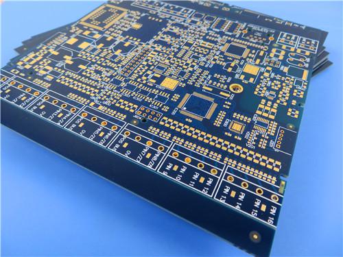
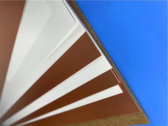
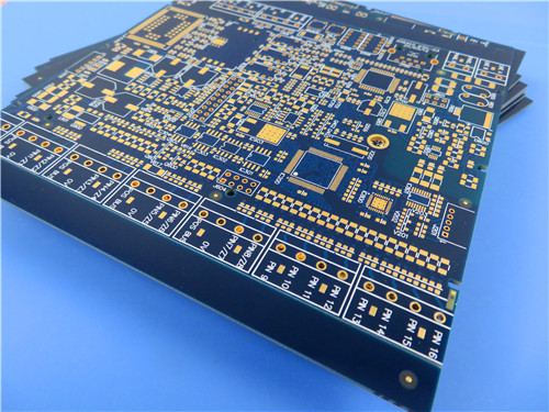
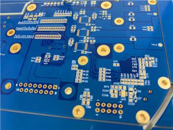
This custom 4-layer hybrid PCB forms a mature differentiated solution by combining domestic low-costF4BM265 PTFE high-frequency material andhigh-Tg S1000-2M epoxy substrate, breaking the single-material performance bottleneck of traditional RF PCBs.
Item NO.:
BIC-586-v671.0Order(MOQ):
1-10Payment:
T/TProduct Origin:
ChinaShipping Port:
ShenzhenLead Time:
7-10 days
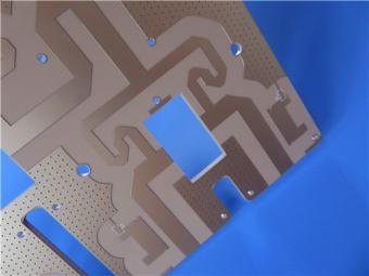
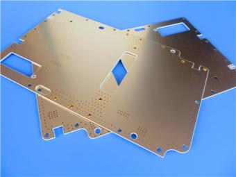
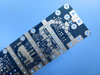
4-Layer F4BM265+S1000-2M Material Hyrbid PCB with Blind Via Impedance Control & ENIG
Product Overview:
This is a our advanced 4-layer hybrid printed circuit board, designed for high-frequency and high-reliability applications. By integrating the superior electrical performance of a PTFE-based laminate with the mechanical rigidity and cost-effectiveness of a standard FR-4 material, this mixed dielectric material PCB offers a unique solution for complex system designs. The following sections detail the construction, stack-up, and key features of this product, followed by an in-depth exploration of the core substrate material, the F4BM265.
Part 1: 4-Layer Hybrid High Frequency PCB Product Technical Introduction
1.1 PCB Construction Specifications
This table aggregates all mandatory mechanical, electrical, manufacturing, and surface finish parameters of the finished hybrid PCB, covering material composition, dimensional tolerance, copper thickness, reliability standards, surface treatment, and special design requirements.
|
Parameter |
Specification |
|
Base Material |
F4BM265 + S1000-2MB |
|
Layer Count |
4 Layers |
|
Board Dimensions |
245mm × 245mm = 1PCS |
|
Finished Board Thickness |
4.14mm |
|
Finished Copper Weight |
35μm per layer |
|
Via Plating Thickness |
25μm |
|
Surface Finish |
ENIG |
|
Top Silkscreen |
White |
|
Bottom Silkscreen |
White |
|
Top Solder Mask |
Blue |
|
Bottom Solder Mask |
Blue |
|
Impedance Control |
Required |
|
Electrical Test |
100% test Prior to shipment |
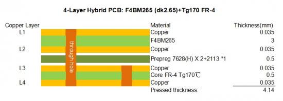
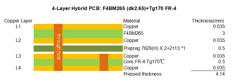
1.2 PCB Layer Stackup Structure
This stack-up displays layer-by-layer vertical stacking sequence from top silkscreen to bottom substrate, clarifying dielectric material types, thickness distribution, and copper layer, serving as the core manufacturing reference for lamination and impedance simulation.
1.3 Core Product Differentiation & Technical Advantages
Pure PTFE thick substrates suffer severe thermal expansion warpage after multi-layer pressing, while single FR4 cannot meet microwave low-loss requirements. This 4-layer design innovatively adopts3mm thick F4BM265 as the top RF signal core to maintain ultra-low dielectric loss at 10–20GHz, paired with0.5mm S1000-2M high-Tg FR4 inner core and S1000-2MB prepreg as bonding medium. S1000-2M features Tg=180°C and ultra-low Z-axis CTE, effectively offsetting the large thermal expansion coefficient of PTFE material, controlling overall board warpage within assembly tolerance range, and realizing the dual performance of RF low-loss and mechanical dimensional stability.
25μm hole copper thickness strictly follows IPC-6012 Class 3 aerospace-grade standard, far exceeding consumer electronics Class 2’s 20μm minimum requirement. Blind vias connect L1-L2 and L3-L4 without through-hole damage to continuous ground planes, avoiding impedance discontinuity caused via stubs, which is critical for phased array antenna, power divider and coupler high-frequency signal transmission. All blind via holes undergo full metallization cross-section sampling inspection to guarantee uniform copper deposition inside micro-holes.
All four conductive layers adopt consistent 35μm finished copper thickness, eliminating impedance deviation caused by inconsistent copper weight between inner and outer layers. The hybrid dielectric structure withtwo different DK materials requires pre-stack impedance simulation before production, and the factory performs impedance testing on coupon samples to ensure actual impedance error within±10%, meeting the strict signal integrity demand of microwave communication equipment.
Blue LPI solder mask provides superior UV resistance compared to green mask, reducing mask yellowing during long-term high-temperature operation of RF equipment. White silkscreen achieves high visibility marking on dark blue background, convenient for manual assembly and field maintenance. Immersion gold surface finish avoids the oxidation risk of bare copper and HASL tin unevenness; thin gold layer ensures stable radio frequency contact performance without signal attenuation, compatible with SMT reflow and hand soldering processes.
All finished panels implement 100% ICT electrical continuity and isolation testing, focusing on blind via interconnection reliability, ground plane integrity and circuit short-circuit risk. Combined with AOI optical inspection for line width/spacing and mask offset defects, dual testing mechanism ensures zero electrical failure rate of outgoing products, matching the high-reliability positioning of radar, satellite communication and base station antenna equipment.
1.4 Application Scenarios of This Hybrid PCB
This 4-layer F4BM265+S1000-2M hybrid PCB targets mid-to-high frequency microwave RF devices requiring both low-loss signal transmission and mechanical structural stability, including:
The 4.14mm thick board structure is suitable for equipment with certain mechanical assembly strength requirements, while the blind via and impedance control design adapts to compact high-density RF layout schemes.
1.5 PCB Product Conclusion
This custom 4-layer hybrid PCB forms a mature differentiated solution by combining domestic low-cost F4BM265 PTFE high-frequency material and high-Tg S1000-2M epoxy substrate, breaking the single-material performance bottleneck of traditional RF PCBs. From material stackup, copper thickness control, blind via structure, IPC Class 3 reliability standards to surface finish and full electrical testing, all parameters are formulated around high-frequency signal integrity and long-term mechanical stability. The fixed 4.14mm compression thickness, 245×245mm single panel size and double-sided blue mask white silkscreen design realize standardized manufacturing while meeting customized RF circuit demands, with broad application value in microwave communication and radar industrial fields.
Part 2: Supporting CCL Material In-Depth Analysis–F4BM265 PTFE Glass Cloth Copper Clad Laminate
2.1 F4BM265 Material Overview
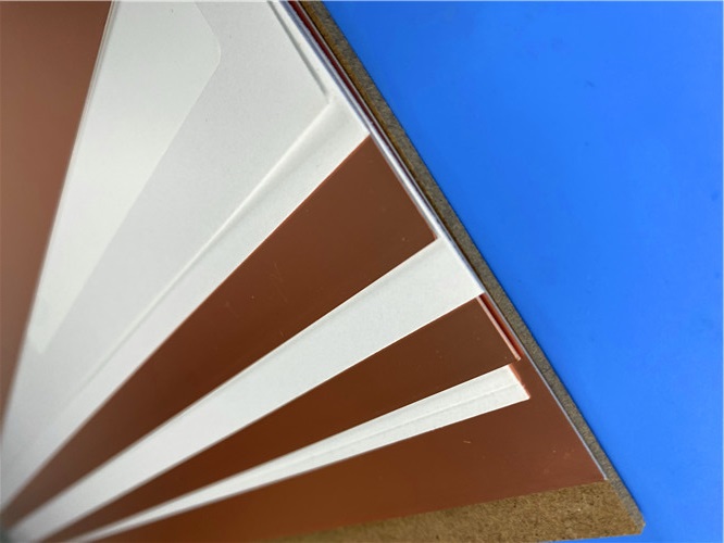
F4BM265 is a domestically mass-produced PTFE woven glass cloth copper-clad laminate independently developed by Wangling Insulation Factory, specially matched for high-frequency hybrid PCB production. It is composed of polytetrafluoroethylene resin, glass fiber woven cloth and ED copper foil, with a fixed dielectric constant DK=2.65 at 10GHz, filling the market gap of mid-DK low-loss domestic RF substrate and replacing imported foreign PTFE laminates. The following content fully sorts out its complete datasheet technical parameters, material composition, core performance characteristics, matching prepreg and copper foil specifications, and production dimensional standards.
2.2 F4BM265 Complete Datasheet Technical Parameter Table
|
Property |
Test Condition |
Unit |
F4BM265 Value |
|
Dielectric Constant (Typical) |
10 GHz |
— |
2.65 |
|
Dielectric Constant Tolerance |
— |
— |
±0.05 |
|
Dissipation Factor (Typical) |
10 GHz |
— |
0.0013 |
|
Dissipation Factor (Typical) |
20 GHz |
— |
0.0019 |
|
Dk Temperature Coefficient |
-55°C to +150°C |
ppm/°C |
-100 |
|
Peel Strength (1 OZ ED Foil) |
F4BM Type |
N/mm |
>1.8 |
|
Peel Strength (1 OZ RTF Foil) |
F4BME Type |
N/mm |
>1.6 |
|
Volume Resistivity |
Normal Condition |
MΩ·cm |
≥6×10⁶ |
|
Surface Resistance |
Normal Condition |
MΩ |
≥1×10⁶ |
|
Electrical Strength |
Z-direction, 5KV, 500V/s |
MV/m |
>25 |
|
Breakdown Voltage |
XY Direction, 5KV, 500V/s |
KV |
>34 |
|
CTE XY |
-55°C to +288°C |
ppm/°C |
14-17 |
|
CTE Z |
-55°C to +288°C |
ppm/°C |
142 |
|
Thermal Stress |
260°C, 10s, 3 cycles |
— |
No Delamination |
|
Water Absorption |
20±2°C, 24 hours |
% |
≤0.08 |
|
Density |
Room Temperature |
g/cm³ |
2.25 |
|
Long-term Service Temperature |
High-Low Temperature Chamber |
°C |
-55 to +260 |
|
Thermal Conductivity |
Z-direction |
W/(M·K) |
0.36 |
|
PIM Value |
F4BME only |
dBc |
≤-159 |
|
Flammability Rating |
— |
UL-94 |
V-0 |
|
Material Composition |
— |
— |
PTFE + Glass Fabric |
|
Copper Foil Type |
— |
— |
ED (F4BM) / RTF (F4BME) |
2.3 F4BM265 Material Composition & Matching Auxiliary Materials
Main raw materials: PTFE resin + woven glass fiber cloth, pressed with scientific proportional mixing. Glass fiber content controls DK value at 2.65; higher glass cloth proportion improves dimensional stability and reduces thermal expansion, while slightly increasing dielectric loss compared tolower DK F4BM series. Standard copper foil matched: ED copper foil (electrodeposited copper), suitable for conventional RF circuits without strict PIM requirements, consistent with the 35μm finished copper design of this4-layer PCB. For passive intermodulation sensitive equipment, F4BME variant with reverse RTF copper foil is optional.
The hybrid PCB adopts S1000-2MB prepreg as the bonding medium between F4BM265 and S1000-2M core. S1000-2M is high-Tg epoxy FR4 substrate with Tg=180℃, low Z-axis CTE and outstanding anti-CAF performance; its epoxy prepreg has strong adhesion to both PTFE and FR4 materials, effectively eliminating interlayer delamination risk during high-temperature lamination of hybrid boards, and solving the warpage defect of thick single PTFE substrates.
Factory standard copper foil options: 0.5oz (18μm), 1oz (35μm), 1.5oz (50μm), 2oz (70μm). This PCB uniformly selects 1oz (35μm) copper foil for all four layers, matching the factory’s standard copper thickness of F4BM265, which avoids custom copper foil surcharges and maintains consistent impedance reference plane thickness.
2.4 F4BM265 Standard Size & Thickness Production Capacity
Standard dielectric thickness list:
0.1mm, 0.127mm, 0.2mm, 0.25mm, 0.5mm, 0.8mm, 1.0mm, 1.5mm, 2.0mm, 2.5mm, 3.0mm, 4.0mm, 5.0mm up to 12mm.
The PCB uses 3.0mm thick F4BM265 core, which belongs to mass-produced standard thickness with tolerance±0.09mm, fully matching the 4.14mm finished board thickness after lamination with S1000-2M 0.5mm core and prepreg.
Regular factory sheet sizes:
460×610mm
500×600mm
850×1200mm
914×1220mm
1000×1200mm
Custom special sizes support 245×245mm single panel required by this product, complying with the factory’s small-size custom processing capacity. Restriction note: substrates with thickness≥4.0mm or≤0.2mm cannot exceed 500×610mm, while 3mm F4BM265 core has no size limitation conflict.
2.5 Core Advantages of F4BM265 Compared with Similar RF Substrates
Fully domestic mass production, lower material and processing cost than imported foreign PTFE laminates of the same DK grade, suitable for medium-batch microwave communication equipment cost control.
DK=2.65 maintains stable dielectric constant from 1GHz to 20GHz, DF only rises from 0.0013 to 0.0019 at 20GHz, suitable for multi-band composite RF circuit design.
Compatible with standard PCB lamination, drilling, etching, surface finish and blind via manufacturing processes, no special customized equipment required for hybrid pressing with FR4 materials.
-55℃to +260℃continuous service temperature, UL94 V-0 flame retardant, low water absorption and anti-radiation performance, applicable to outdoor base stations, vehicle-mounted radar and aerospace equipment.
2.6 Typical Applications for F4BM265
2.7 F4BM265 CCL Material Conclusion
As a mid-DK low-loss domestic PTFE glass cloth copper-clad laminate, F4BM265 provides a cost-effective high-frequency material solution for hybrid PCB design. Its standardized DK=2.65 ultra-low dielectric loss characteristic meets the core electrical demand of microwave RF circuits, while complete supporting thickness, size and copper foil options support flexible hybrid stack matching with high-Tg S1000 series FR4 substrates. Combined with stable thermal stress resistance, low water absorption and wide temperature adaptability, it perfectly matches the technical requirements of the 4-layer blind via impedance-controlled ENIG hybrid PCB described above, serving as the core material foundation to balance RF electrical performance and mechanical reliability of finished boards, and has wide popularization value in domestic communication and radar high-frequency equipment manufacturing industry.
Previous:
8-Layer Hybrid PCB RO4003C + S1000-2M FR4 with ENIG Surface Finish Blind ViaNext:
4-Layer Wangling WL-CT338 + FR4 Hybrid PCB ENIG Green Solder Mask White SilkscreenIf you have questions or suggestions,please leave us a message,we will reply you as soon as we can!
Categories
New Products
Wangling F4BTMS220 2-Layer DK2.2 PCB 10 mil Core with Immersion Gold
Wangling F4BTME350 10mil DK3.5 High Frequency Substrate PCB 2-Layer Immersion Gold
Wangling F4BTM300 Custom 2-layer PCB 20mil DK3.0 Substrate with Immersion Gold
Rogers 20mil RT/duroid 6202 2-layer ENIG High-Frequency Microwave PCB
Rogers 20mil AD250C PCB Pure Gold High-Frequency Antenna Circuit Board
8-Layer Hybrid RF PCB: RO4350B + TG170 FR-4 + RO4003C with RO4450F Bondply
4-Layer Rogers RO3010 Hybrid PCB Immersion Silver 2.8mm Finished Thickness
4-Layer 20mil Rogers RO3210 ISIG High-Frequency PCB with Controlled Depth Milling
RO4003C exhibit a stable dielectric constant over a broad frequency range. This makes it an ideal substrate for broadband applications. And signal integrity performance improvement over the stack-ups with all FR4 board.
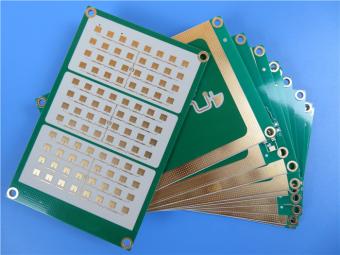
The hybrid PCB can be a mixture of FR-4 and high frequency material, and a mixture of high frequency material with different dielectric constant (DK)
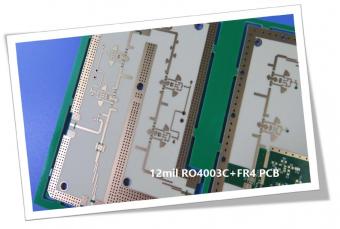
The 12mil core is on the top layer and it mainly plays the roles of signal layer. The core has fixed thickness which is very important to the electrical length of RF lines on the circuit board.
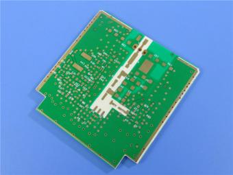
The hybrid PCB can be a mixture of FR-4 and high frequency material as abovementioned.
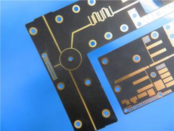
It contains 2 different boards in the panel. PCB boards are manufactured strictly as per required specifications with the standard IPC-Class-II.
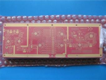
Hybrid PCB is also known as mixed material lamination, it’s normally combined by two different material like FR4 and PI(rigid flex PCB), FR4 and Ceramic, FR4 and Teflon, FR4 and Aluminum base etc.
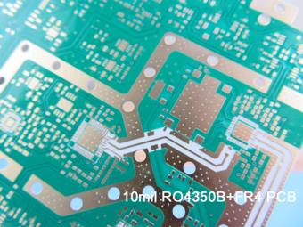
Hybrid constructions PCB typically involve a low loss material such as Nelco or Rogers combined with another core material like FR-4.
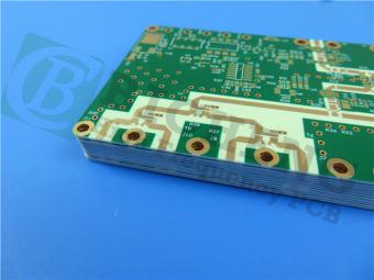
The Hybrid PCB on RO3003 and High Tg FR-4 is a state-of-the-art solution for high-frequency applications. With its exceptional stability, reliability, and manufacturability, it caters to the demands of industries such as automotive, telecommunications, and satellite communications.
 6-11C Shidai Jingyuan, Fuyong, Baoan, Shenzhen, Guangdong, China 518103


For inquiries about our products or pricelist, please leave to us and we will be in touch within 24 hours.
© Copyright: 2026 Shenzhen Bicheng Electronics Technology Co., Ltd.. All Rights Reserved.

IPv6 network supported


