

 Call Us Now !
Tel : +86 755 27374946
Call Us Now !
Tel : +86 755 27374946
 Order Online Now !
Email : info@bichengpcb.com
Order Online Now !
Email : info@bichengpcb.com
The TP2000 high frequency PCB 6mm Pure Gold represents a specialized, high-reliability product for engineers who require extreme electrical performance in a mechanically robust format.
Item NO.:
BIC-551-v636.0Order(MOQ):
1-10Payment:
T/TProduct Origin:
ChinaShipping Port:
ShenzhenLead Time:
7-10 days
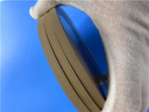
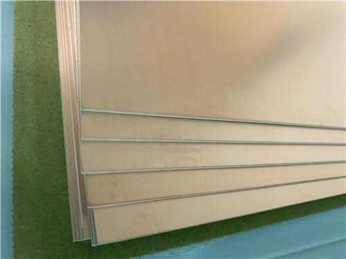
TP2000 PCB TP Series 6mm Wangling DK20 Substrate Pure Gold Bare Copper
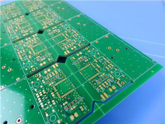
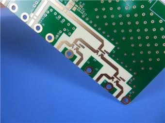
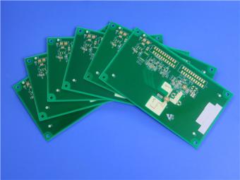
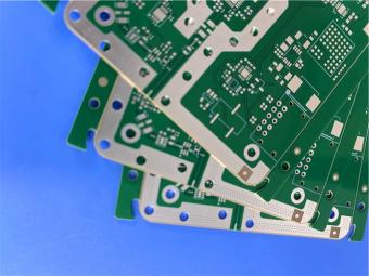
TP2000 PCB 6mm Pure Gold, a high-performance 2-layer rigid printed circuit board purpose-built for extreme RF, microwave, aerospace, radar, and satellite communication systems. It combines ultra-high dielectric constant, ultra-low loss, exceptional thermal stability, and robust mechanical integrity in a thick-core, high-reliability construction optimized for compact, high-signal-integrity designs.
1. Product Overview
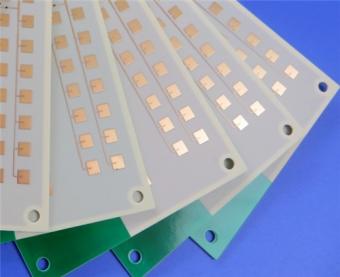
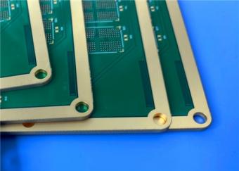
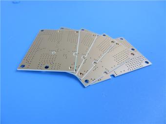
The TP2000 6mm Pure Gold PCB is a specialized high-frequency rigid circuit board built on a 6mm TP2000 thermoplastic dielectric core, double-clad with 1oz (35μm) electrolytic ductile (ED) copper. Engineered without solder mask or silkscreen, it prioritizes raw radio-frequency performance, dimensional stability, and thermal consistency. The“Pure Gold”designation reflects its premium material formulation, precision fabrication, and noble electrical characteristics rather than a surface plating; the board uses bare copper as the final finish to preserve high-frequency signal transparency and minimize insertion loss.
This DK20 PCB is not a general-purpose commercial board. It is designed for applications where signal purity, miniaturization, wide-temperature resilience, and long-term reliability are non-negotiable. Its 6mm thick core provides exceptional structural rigidity, making it suitable for standalone substrates, antenna radiators, and high-voltage / high-power circuit carriers.

2. PCB Construction
The following table consolidates all mechanical, fabrication, and layout parameters that define the board’s physical build.
|
Parameter |
Specification |
|
Board Dimensions |
85mm × 85mm (1 piece), tolerance ±0.15mm |
|
Minimum Trace / Space |
6 / 7 mils |
|
Minimum Hole Size |
0.35mm |
|
Blind Vias |
Not allowed |
|
Finished Board Thickness |
6.1mm |
|
Finished Copper Weight (Outer Layers) |
1oz (1.4 mils / 35μm) |
|
Via Plating Thickness |
20μm |
|
Surface Finish |
Bare copper |
|
Top Silkscreen |
No |
|
Bottom Silkscreen |
No |
|
Top Solder Mask |
No |
|
Bottom Solder Mask |
No |
|
Electrical Test |
100% full electrical test before shipment |
3. PCB Stackup
This symmetric 2-layer stackup delivers balanced electrical performance, mechanical stability, and low warpage under thermal cycling.
|
Layer |
Material |
Thickness |
|
Outer Layer 1 |
Copper foil |
35μm |
|
Core Dielectric |
TP2000 high frequency thermoplastic |
6.0mm |
|
Outer Layer 2 |
Copper foil |
35μm |
|
Total Finished Thickness |
— |
6.1mm |
4. PCB Layout Statistics
This table quantifies component, pad, via, and net complexity for design verification and assembly planning.
|
Item |
Quantity |
|
Total Components |
24 |
|
Total Pads |
37 |
|
Through Hole Pads |
18 |
|
Top SMT Pads |
19 |
|
Bottom SMT Pads |
0 |
|
Vias |
12 |
|
Electrical Nets |
2 |
TP2000 Copper-Clad Laminate (CCL)–Complete Material Knowledge Base
This section is fully separated from the WanglingTP2000 PCB description and provides in-depth material science, specifications, and application guidance for TP2000 high-frequency CCL.
1. Material Introduction
TP2000 is a proprietary high-frequency thermoplastic copper-clad laminate designed specifically for RF, microwave, and millimeter-wave circuits. Its dielectric layer consists of a ceramic-filled polyphenylene oxide (PPO) resin matrix with no fiberglass reinforcement, enabling exceptional dielectric uniformity, low loss, and precise Dk control. By adjusting the ceramic-to-resin ratio, manufacturers can customize Dk from 3.0 to 25; the standard TP2000 grade is fixed at Dk = 20±0.8 for extreme miniaturization.
Unlike ceramic substrates, TP2000PCB substrate offers superior mechanical toughness, easier machining, and lower cost. Unlike PTFE-based materials, it features better dimensional stability, stronger copper adhesion, and compatibility with standard PCB fabrication processes. It carries UL 94-V0 flammability rating, ensuring safety in enclosed electronic systems.
The TP series includes:

2.Datasheet Table–TP2000 CCL
|
Property |
Test Condition |
Unit |
TP2000 Value |
|
Dielectric constant (Dk) |
5 GHz, stripline method |
– |
20.0 ± 0.8 (custom 3–25) |
|
Dk tolerance |
– |
% |
±4% |
|
Dissipation factor (Df) |
5 GHz |
– |
0.0020 – 0.0025 |
|
Temperature coefficient of Dk (TCDk) |
–55 °C to +150 °C |
ppm/°C |
–55 |
|
Peel strength (1 oz copper) |
Normal condition |
N/mm |
> 0.6 |
|
Peel strength (1 oz copper) |
After humidity cycling |
N/mm |
> 0.4 |
|
Volume resistivity |
500 V, normal |
MΩ·cm |
> 1 × 10⁹ |
|
Surface resistivity |
500 V, normal |
MΩ |
> 1 × 10⁷ |
|
CTE (X-axis) |
–55 °C to +150 °C |
ppm/°C |
35 |
|
CTE (Y-axis) |
–55 °C to +150 °C |
ppm/°C |
35 |
|
CTE (Z-axis) |
–55 °C to +150 °C |
ppm/°C |
40 |
|
Water absorption |
20±2 °C, 24 hours |
% |
≤ 0.01 |
|
Long term operating temperature |
– |
°C |
–100 to +150 |
|
Density |
23 °C |
g/cm³ |
2.73 |
|
Flammability |
UL94 |
class |
V 0 |
|
Material Composition |
– |
– |
Ceramic + PPO resin, ED Cu |
3.Key Material Advantages
1)Ultra-High Dk for Extreme Miniaturization: Dk=20 allows antenna and passive component sizes to be reduced dramatically compared to standard Dk=3–6 materials.
2)Ultra-Low Loss Across Wide Bandwidth: Df remains stable below 10GHz, supporting broadband systems.
3)Excellent Thermal Stability: TCDK and controlled CTE preserve electrical and mechanical performance under thermal shock.
4)Superior Radiation Resistance & Low Outgassing: Ideal for space, avionics, and military systems.
5)Strong Copper Adhesion: More reliable than vacuum-deposited coatings on ceramic substrates.
6)Ease of Machining: Drills, mills, and cuts cleanly without chipping—unlike brittle ceramics.
7)Cost Efficiency: Lower fabrication cost than ceramic substrates while exceeding performance of many thermoset materials.
4.Processing & Assembly Guidelines
1)Multilayer Design: Generally not recommended due to thermoplastic behavior; if required, use low-temperature bonding films with full feasibility validation.
2)Soldering: Avoid wave solder and standard reflow (260°C). Use manual constant-temp soldering. If reflow is mandatory, limit peak temperature to≤200°C.
3)Etching & Plating: Compatible with standard PCB processes; ensure thermal profiles remain within material limits.
4)Testing: Supports IPC-TM-650 and GB/T test methods for dielectric, mechanical, and thermal validation.
5)Thickness Range: Standard 0.5mm–12.0mm; 6.0mm with tight tolerance available.
6)Standard Sizes: 150×150, 160×160, 200×200, 170×240mm; custom sizes available.
5.Typical Applications
TP2000 PCB laminate is the material of choice for:
Conclusion
The TP2000 high frequency PCB 6mm Pure Gold represents a specialized, high-reliability product for engineers who require extreme electrical performance in a mechanically robust format. The combination of a 6 mm thick ceramic-filled core, pure gold finish, and ultra-low loss tangent makes it unmatched for compact, high-frequency systems operating in harsh environments. The companion TP2000 PCB material offers a versatile, machinable alternative to brittle ceramic substrates while maintaining superior dielectric stability from -100°C to +150°C.


Previous:
TP1600 PCB 31.49mil High DK16 Wangling Laminate Pure Gold PlatingNext:
25mil TF600-Based 2-Layer DK6.0 TF Series PCB with ENIG and Copper-filled ViasIf you have questions or suggestions,please leave us a message,we will reply you as soon as we can!
Categories
New Products
12-layer TG200 TU-872 SLK High-Speed FR4 1.68mm PCB with ENIG Impedance Control
12-Layer RO4350B + RO3010 3.14mm Hybrid PCB Nickel-Free EPIG Surface Finish Blind Via
8-Layer Hybrid PCB RO4003C + S1000-2M FR4 with ENIG Surface Finish Blind Via
6-Layer Isola Astra MT77 PCB with Blind Via & Resin Plug Immersion Silver Finish
2-Layer 20mil FSD1020T ENIG High-Frequency PCB with Via Resin Plugged and Capped
4-Layer F4BM265+S1000-2M Material Hyrbid PCB with Blind Via Impedance Control & ENIG
4-Layer Wangling WL-CT338 + FR4 Hybrid PCB ENIG Green Solder Mask White Silkscreen
6-layer Isola 370HR High-Tg FR-4 PCB 2μ" ENIG Impedance Controlled
Polytetrafluoroethylene (Short for PTFE), commonly known as "plastic king ", is a polymer compound made of tetrafluoroethylene by polymerization. It has excellent chemical stability, corrosion resistance, sealing, high lubrication and non-viscosity, electrical insulation and good aging resistance.
Rogers TMM4 thermoset microwave material is ceramic, hydrocarbon, thermoset polymer composite designed for high plated-through-hole reliability stripline and microstrip applications.
Taconic TLY laminates are a type of low loss laminates. They are manufactured with very light weight woven fiberglass and are more dimensionally stable than chopped fiber reinforced PTFE composites.
RO3203 laminates combine the surface smoothness of a non-woven PTFE laminate, for finer line etching tolerances, with the rigidity of a woven-glass PTFE laminate. These materials can be fabricated into printed circuit boards using
This type of immersion silver RF PCB is made on one of Taconic’s ORCER family material: RF-45.
Rogers’ TMM10 thermoset microwave materials are ceramic, hydrocarbon, thermoset polymer composites designed for high plated-thru-hole reliability stripline and microstrip applications.
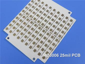
Rogers RO3006 was designed to offer exceptional electrical and mechanical stability at competitive prices.
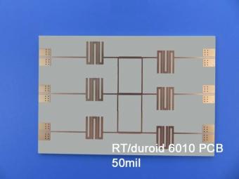
RT/duroid 6010LM microwave laminates feature ease of fabrication and stability in use. This property results in the possibility of mass production and reducing the cost of goods.
 6-11C Shidai Jingyuan, Fuyong, Baoan, Shenzhen, Guangdong, China 518103


For inquiries about our products or pricelist, please leave to us and we will be in touch within 24 hours.
© Copyright: 2026 Shenzhen Bicheng Electronics Technology Co., Ltd.. All Rights Reserved.

IPv6 network supported


