

 Call Us Now !
Tel : +86 755 27374946
Call Us Now !
Tel : +86 755 27374946
 Order Online Now !
Email : info@bichengpcb.com
Order Online Now !
Email : info@bichengpcb.com
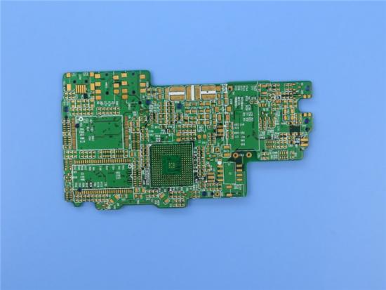
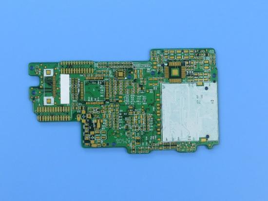
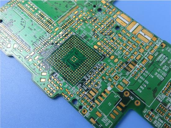
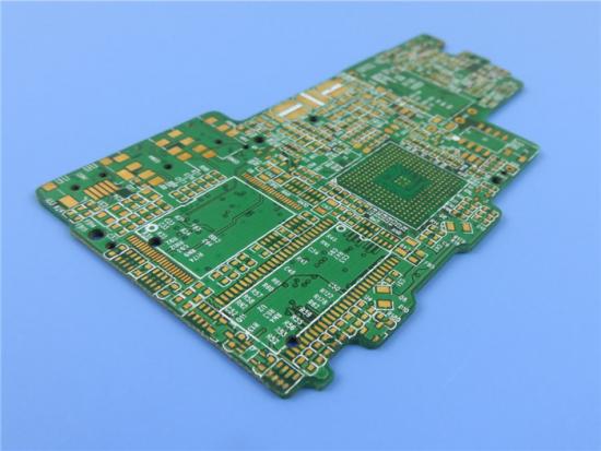
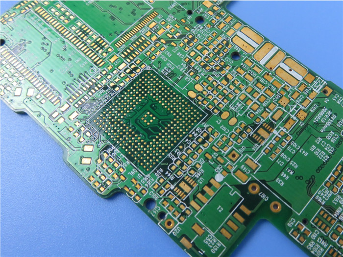
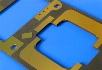
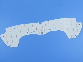
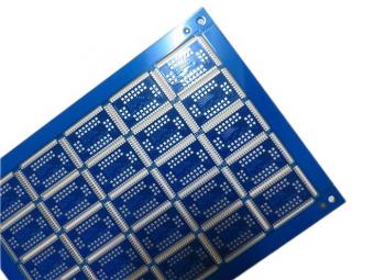
This is a type of multilayer PCB built on FR-4 substrate with Tg 150°C for the application of mobile phone with blind via technology.
Item NO.:
BIC-452-v73.0Order(MOQ):
1-10Payment:
T/TProduct Origin:
ChinaShipping Port:
ShenzhenLead Time:
7-10 daysBlind Via PCB Built on Tg150℃ FR-4 With Immersion Gold 4-Layer FR-4 Circuit Board
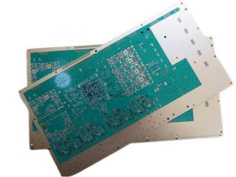
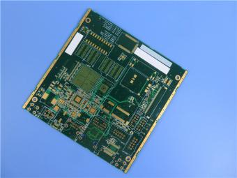
(Printed circuits boards are custom-made products, the picture and parameters shown are just for reference)
1.1 General description:
It's 1.6 mm thick with white silkscreen(Taiyo) on green solder mask (Taiyo) and immersion gold on pads. The base material is from ITEQ supplying single up PCB. They're fabricated per IPC 6012 Class 2 using supplied Gerber data. Each 25 boards are packed for shipment.
1.2 Features and Benefits :
1.2.1 Middle Tg FR-4 Shows low Z-CTE and excellent through hole reliability;
1.2.2 Immersion gold has high solderability, no stressing and less contamination;
1.2.3 Multilayer shortened connection between electronic components;
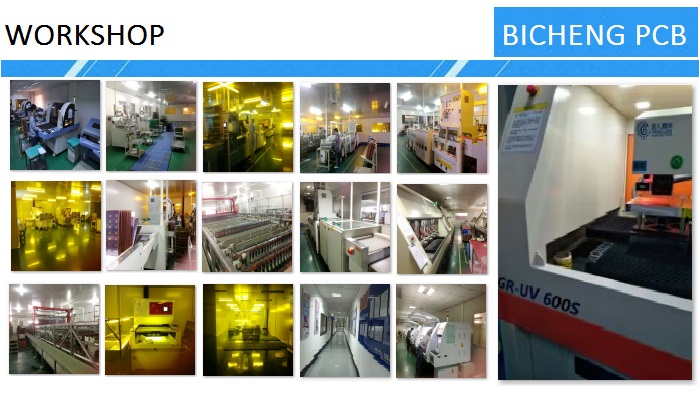
1.2.4 16000㎡workshop and 8000 types of PCB's per month;
1.2.5 Delivery on time: >98%
1.2.6 No minimum order quantity. 1 piece is available;

1.3 Applications:
Industrial Computer
GPS Tracking System
POS Cash Register
Embedded Systems
Data Acquisition System
Microcontrollers
PC and Notebook
1.4 Parameter and data sheet:
| PCB SIZE | 119 x 80mm=1PCS |
| BOARD TYPE | Multilayer PCB |
| Number of Layers | 4 layers |
| Surface Mount Components | YES |
| Through Hole Components | YES |
| LAYER STACKUP | copper ------- 18um(0.5oz)+plate TOP layer |
| Core FR-4 0.61mm | |
| copper ------- 35um(1oz) MidLayer 1 | |
| Prepreg 0.254mm | |
| copper ------- 35um(1oz) MidLayer 2 | |
| Core FR-4 0.61mm | |
| copper ------- 18um(0.5oz)+plate BOT layer | |
| TECHNOLOGY | |
| Minimum Trace and Space: | 4 mil / 4 mil |
| Minimum / Maximum Holes: | 0.3 mm /3.5 mm |
| Number of Different Holes: | 9 |
| Number of Drill Holes: | 415 |
| Number of Milled Slots: | 0 |
| Number of Internal Cutouts: | 0 |
| Impedance Control: | no |
| Number of Gold finger: | 0 |
| BOARD MATERIAL | |
| Glass Epoxy: | FR-4 Tg150℃, er<5.4.IT-158, ITEQ |
| Final foil external: | 1oz |
| Final foil internal: | 1oz |
| Final height of PCB: | 1.6mm ±0.16 |
| PLATING AND COATING | |
| Surface Finish | Immersion Gold |
| Solder Mask Apply To: | TOP and Bottom, 12micron Minimum |
| Solder Mask Color: | Green, PSR-2000 GT600D, Taiyo Supplied. |
| Solder Mask Type: | LPSM |
| CONTOUR/CUTTING | Routing, stamp holes. |
| MARKING | |
| Side of Component Legend | TOP and Bottom. |
| Colour of Component Legend | White, S-380W, Taiyo Supplied. |
| Manufacturer Name or Logo: | Marked on the board in a conductor and leged FREE AREA |
| VIA | Plated through hole(PTH), minimum size 0.3mm. Blind Via Top to Inner layer 1, Bottom to Inner layer 2 |
| FLAMIBILITY RATING | UL 94-V0 Approval MIN. |
| DIMENSION TOLERANCE | |
| Outline dimension: | 0.0059" |
| Board plating: | 0.0029" |
| Drill tolerance: | 0.002" |
| TEST | 100% Electrical Test prior shipment |
| TYPE OF ARTWORK TO BE SUPPLIED | email file, Gerber RS-274-X, PCBDOC etc |
| SERVICE AREA | Worldwide, Globally. |
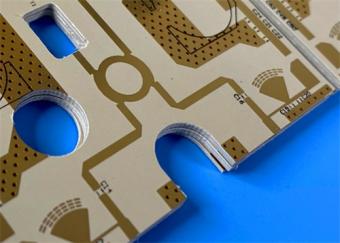
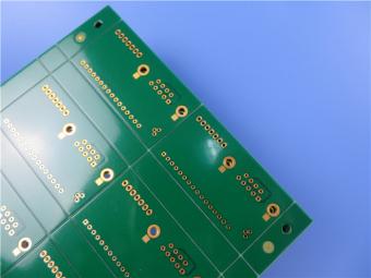
1.5 Composition of Holes:
The blind hole is located on the top and bottom surface of the printed circuit board and has a certain depth for the connection between the surface line and the inner line below. The depth of the hole usually does not exceed a certain ratio (aperture). Buried hole is a connecting hole located in the inner layer of the printed circuit board, which does not extend to the surface of the circuit board.
The above two kinds of holes are located in the inner layer of the circuit board. The formation of through hole process is used before lamination, and several inner layers may be overlapped done during the formation of the through hole.
The third is called a through hole, which passes through the entire circuit board. It can be used to interconnect internally or as an installation location hole for components. Because the through hole is easier to realize and the cost is low, it is used in most printed circuit boards instead of the other two. The following mentioned holes, without special instructions, are considered as through holes.
From the design point of view, a hole is mainly composed of two parts, one is the middle hole (drill hole), the other is the pad area around the hole, see below. The size of these two parts determines the size of the hole. Clearly, in
high-speed, high-density PCB design, designers always want the holes the smaller the better, so that it can leave more wiring space on the board.

BICHENG MAIN COURIERS:

Previous:
Impedance Controlled 12 Layers High Tg HDI Multilayer FR-4 PCB BoardNext:
Thin PCB 0.2mm FR-4 Printed Circuit Board with White Solder Mask OSPIf you have questions or suggestions,please leave us a message,we will reply you as soon as we can!
Categories
New Products
30mil Taconic CER-10 2-layer Immersion Silver DK10 High Frequency Laminate PCB
31mil Rogers RT/duroid 5880 Double-sided Bare Copper ENIG Finished PCB
Wangling TFA294 Laminate 40mil Immersion Silver No Solder Mask Silkscreen Custom PCB
50mil TMM6 PCB 2-layer EPIG Rogers DK6.0 Substrate No Solder Mask Silkscreen
60mil TMM10 PCB 1-layer OSP Microwave High Frequency Laminate No Solder Mask
Wangling F4BTMS265 Custom PCB 30mil 2-layer ENIG Black Solder Mask White Silkscreen
RO4835 20mil Rogers Laminate 2-layer Immersion Gold Custom PCB
Rogers 20mil DiClad 527 PCB 2-layer Immersion Gold No Solder Mask Black Silkscreen
This is a type of single sided circuit board built on FR-4 substrate with CTI 600V.
It’s a very simple board with white solder mask and OSP on pads.
This is a type of impedance controlled PCB built on FR-4 material with Tg 175°C for the application of Signal transmission.
TU-872 SLK Sp is based on a high performance modified epoxy FR-4 resin. This material is reinforced with novel woven glass and designed with extra low dielectric constant and low dissipation factor for high speed low loss and high frequency circuit board application.
This is a type of standard double sided high temperature PCB which is built on ITEQ’s IT-180ATC laminate.
This is a type of multi-layer PCB built on FR-4 substrate with Tg 135°C for the application of digital receivers.
This is a type of double sided circuit board built on FR-4 substrate with Tg 170°C for the application of keypad.
This is a type of heavy copper PCB built on FR-4 substrate with Tg 135°C for the application of UPS systems.
 6-11C Shidai Jingyuan, Fuyong, Baoan, Shenzhen, Guangdong, China 518103


For inquiries about our products or pricelist, please leave to us and we will be in touch within 24 hours.
© Copyright: 2026 Shenzhen Bicheng Electronics Technology Co., Ltd.. All Rights Reserved.

IPv6 network supported


