

 Call Us Now !
Tel : +86 755 27374946
Call Us Now !
Tel : +86 755 27374946
 Order Online Now !
Email : info@bichengpcb.com
Order Online Now !
Email : info@bichengpcb.com
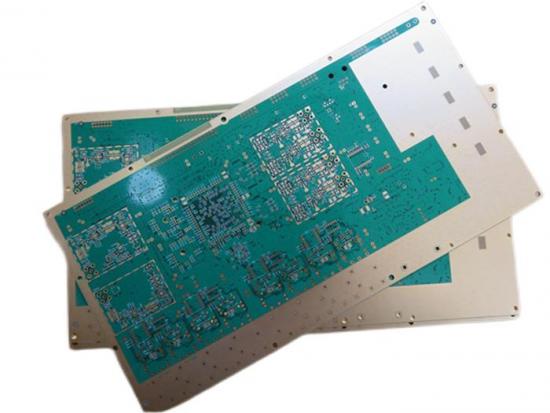
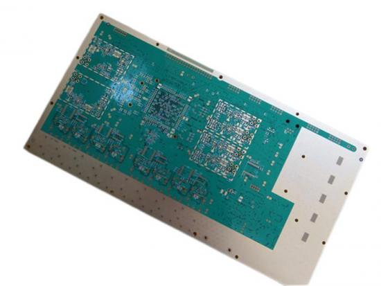
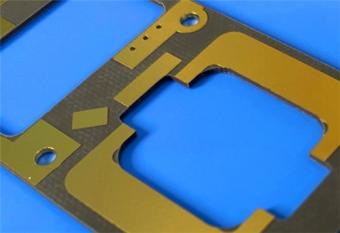
This is a type of impedance controlled PCB built
on FR-4 material with Tg 175°C for the application of Signal transmission.
Item NO.:
BIC-476-v74.0Order(MOQ):
1-10Payment:
T/TProduct Origin:
ChinaShipping Port:
ShenzhenLead Time:
7-10 days
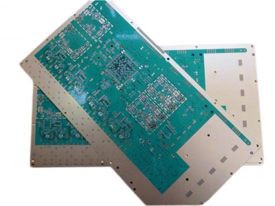
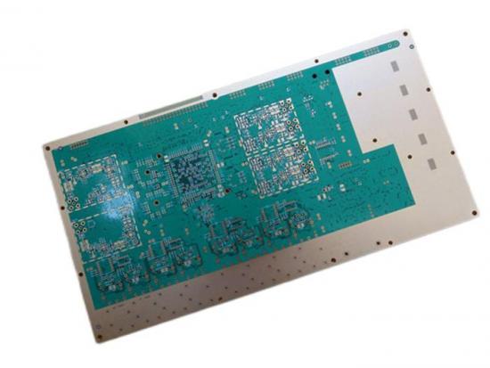
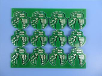
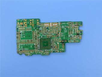
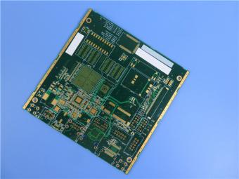
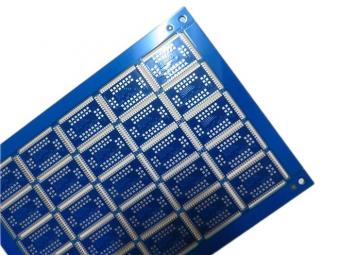
Impedance Controlled PCB 12 Layers High Tg Printed Circuit Board HDI Multilayer PCB Board On 2.0mm FR-4
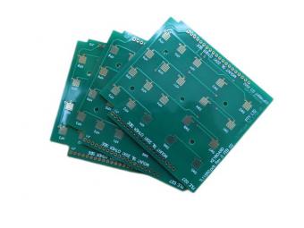
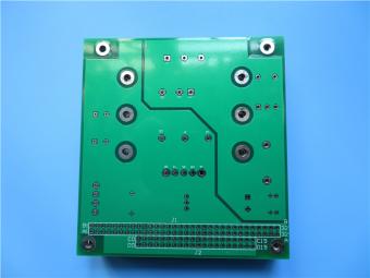
(Printed Circuit Boards are custom-made products, the picture and parameters shown are just for reference)
1.1 General description
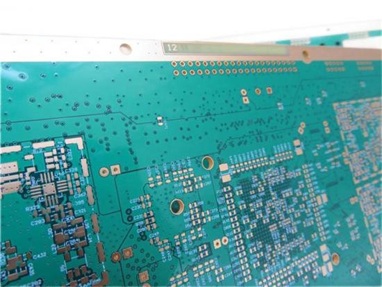
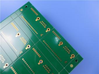
It's a 12-layer board with 2.0 mm thick. It contains 2+N+2 HDI vias (see the stackup & vias). White silkscreens (Taiyo) are on green solder mask (Taiyo) and immersion gold on pads. Both Signal trace impedance and differential pairs impedance are controlled on layers. See the drawing below. The base material is from ITEQ. Entire panel is supplying with single up. They're fabricated per IPC 6012 Class 2 using supplied Gerber data. Each 20 boards are packed for shipment.
| Signal Trace Impedance Control | ||||
| Trace Layer | Trace Width (mil) | Trace Impedance (Ohm) | Precision | Reference Layer |
| Top Layer | 4 | 50 | ±10% | Mid-Layer 1 |
| L03, Mid-Layer 2 | 4 | 50 | ±10% | Mid-Layer 1 |
| L10, Mid-Layer 9 | 4 | 50 | ±10% | Mid-Layer 7, Mid-Layer 10 |
| Bottom Layer | 4 | 50 | ±10% | Mid-Layer 10 |
| Differential Pairs Impedance Control | ||||
| Layer | Trace Width / Space (Mil) | Trace Impedance (Ohm) | Precision | Frequency (MHz) |
| Top Layer | 3.1 / 5.5 | 100 | ±10% | Mid-Layer 1 |
| Top Layer | 4.0 / 5.1 | 90 | ±10% | Mid-Layer 1 |
| L03, Mid-Layer 2 | 3.1 / 5.9 | 100 | ±10% | Mid-Layer 1, Mid-Layer 4 |
| L06, Mid-Layer 5 | 4.0 / 7.4 | 100 | ±10% | Mid-Layer 4, Mid-Layer 6 |
| L06, Mid-Layer 5 | 4.0 / 4.7 | 90 | ±10% | Mid-Layer 4, Mid-Layer 6 |
| L07, ,Mid-Layer 6 | 4.0 / 7.4 | 100 | ±10% | Mid-Layer 5, Mid-Layer 7 |
| L07, ,Mid-Layer 6 | 4.0 / 4.7 | 90 | ±10% | Mid-Layer 5, Mid-Layer 7 |
| L10, Mid-Layer 9 | 3.1 / 5.9 | 100 | ±10% | Mid-Layer 7, Mid-Layer 10 |
| Bottom Layer | 4.0 / 5.5 | 100 | ±10% | Mid-Layer 10 |
| Bottom Layer | 4.0 / 5.1 | 90 | ±10% | Mid-Layer 10 |
1.2 Features and benefits
Lead free assemblies with a maximum reflow temperature of 260℃.
Long storage time ( It can be stored for more than 1 year in vacuum bag)
Improved the speed of signal transmission
PCB manufacturing on required specifications.
Quick and on-time delivery
UL recognized and RoHS Directive-compliant
Prototype PCB capability

1.3 Applications
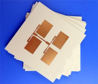
Dsl Modem
Solar Battery Charger
Vehicle Tracker
GPS Receiver
Wi Fi Antenna
Bluetooth USB Hub
USB Wireless Router
SMS Modem
Multicoupler Antenna
Phone systems
1.4 Parameter and data sheet
| PCB SIZE | 257 x 171.5mm=1PCS=1design |
| BOARD TYPE | Multilayer PCB |
| Number of Layers | 12 Layers |
| Surface Mount Components | YES |
| Through Hole Components | YES |
| LAYER STACKUP | copper ------- TOP 17um(1oz)+plate 25um |
| 130 um prepreg 1080 x 2 | |
| copper ------- L02 32um(1oz) | |
| 150um core FR-4 | |
| copper ------- L03 18um(0.5oz) | |
| 130 um prepreg 1080 x 2 | |
| copper ------- L04 18um(0.5oz) | |
| 150um core FR-4 | |
| copper ------- L05 18um(0.5oz) | |
| 130 um prepreg 1080 x 2 | |
| copper ------- L06 18um(0.5oz) | |
| 813um core FR-4 | |
| copper ------- L07 18um(0.5oz) | |
| 130 um prepreg 1080 x 2 | |
| copper ------- L08 18um(0.5oz) | |
| 150um core FR-4 | |
| copper ------- L09 18um(0.5oz) | |
| 130 um prepreg 1080 x 2 | |
| copper ------- L10 18um(0.5oz) | |
| 150um core FR-4 | |
| copper ------- L11 35um(1oz) | |
| 130 um prepreg 1080 x 2 | |
| copper ------- BOT 17um(0.5oz)+plate 25um | |
| TECHNOLOGY | |
| Minimum Trace and Space: | 4 mil / 4 mil |
| Minimum / Maximum Holes: | 0.25 mm / 3.0 mm |
| Number of Different Holes: | 26 |
| Number of Drill Holes: | 4013 |
| Number of Milled Slots: | 0 |
| Number of Internal Cutouts: | 0 |
| Impedance Control | Single Signal Impedance and Differential Pairs Impedance |
| BOARD MATERIAL | |
| Glass Epoxy: | FR-4, ITEQ IT-180, Tg>175℃, er<5.4 |
| Final foil external: | 1oz |
| Final foil internal: | 1oz |
| Final height of PCB: | 2.0mm ±10% |
| PLATING AND COATING | |
| Surface Finish | Immersion Gold (ENIG)( 2 µ" over 100 µ" nickel) |
| Solder Mask Apply To: | Top and Bottom, 12micon Minimum. |
| Solder Mask Color: | Green, PSR-2000GT600D, Taiyo supplied. |
| Solder Mask Type: | LPSM |
| CONTOUR/CUTTING | Routing |
| MARKING | |
| Side of Component Legend | TOP |
| Colour of Component Legend | White, IJR-4000 MW300, Taiyo Supplied. |
| Manufacturer Name or Logo: | Marked on the board in a conductor and leged FREE AREA |
| VIA | Plated Through Hole(PTH), via tented. Vin in pad under BGA package |
| FLAMIBILITY RATING | UL 94-V0 Approval MIN. |
| DIMENSION TOLERANCE | |
| Outline dimension: | 0.0059" (0.15mm) |
| Board plating: | 0.0030" (0.076mm) |
| Drill tolerance: | 0.002" (0.05mm) |
| TEST | 100% Electrical Test prior shipment |
| TYPE OF ARTWORK TO BE SUPPLIED | email file, Gerber RS-274-X, PCBDOC etc |
| SERVICE AREA | Worldwide, Globally. |

1.5 Impedance PCB and Impedance Match
The characteristic impedance of the conductor on the printed circuit board is an important indicator of the circuit design, especially in the PCB design of high frequency circuit. Whether the characteristic impedance of the conductor is consistent and matching with the characteristic impedance required by the device or signal must be taken into consideration. Therefore, these two concepts in reliability design of PCB design must be paid attention.
There will be a variety of signal transmission in the conductor of circuit board. To increase the rate of transmission, it must increase its frequency. Due to the factors of the circuit itself such as etching, stack thickness, track width and so on are different, it will cause changes of the impedance value, resulting in its signal distortion. Therefore, the impedance value of conductor on high-speed circuit board should be controlled within a certain range, known as the "impedance control". The factors that affect the impedance of the PCB wiring are mainly the width of the copper track, the thickness of the copper track, the dielectric constant of the dielectric, the thickness of the dielectric, the thickness of the pad, the path of the ground layer, the wires around the wiring, etc. So the impedance of the wiring on the board must be controlled in the design of the PCB to avoid signal reflection and other electromagnetic interference and signal integrity issues as far as possible, to guarantee the stability of the actual use of the PCB board. You can refer to the corresponding empirical formula for the calculation method of micro-strip line and strip line impedance on PCB board.
BICHENG MAIN COURIERS:

Previous:
Low Dk / Df FR-4 High Thermal Reliability Printed Circuit Board TU-872 Multilayer PCBNext:
Blind Via PCB Built on Tg150℃ FR-4 With Immersion Gold 4-LayerIf you have questions or suggestions,please leave us a message,we will reply you as soon as we can!
Categories
New Products
30mil Taconic CER-10 2-layer Immersion Silver DK10 High Frequency Laminate PCB
31mil Rogers RT/duroid 5880 Double-sided Bare Copper ENIG Finished PCB
Wangling TFA294 Laminate 40mil Immersion Silver No Solder Mask Silkscreen Custom PCB
50mil TMM6 PCB 2-layer EPIG Rogers DK6.0 Substrate No Solder Mask Silkscreen
60mil TMM10 PCB 1-layer OSP Microwave High Frequency Laminate No Solder Mask
Wangling F4BTMS265 Custom PCB 30mil 2-layer ENIG Black Solder Mask White Silkscreen
RO4835 20mil Rogers Laminate 2-layer Immersion Gold Custom PCB
Rogers 20mil DiClad 527 PCB 2-layer Immersion Gold No Solder Mask Black Silkscreen
This is a type of single sided circuit board built on FR-4 substrate with CTI 600V.
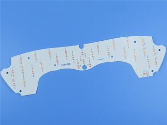
It’s a very simple board with white solder mask and OSP on pads.
This is a type of multilayer PCB built on FR-4 substrate with Tg 150°C for the application of mobile phone with blind via technology.
TU-872 SLK Sp is based on a high performance modified epoxy FR-4 resin. This material is reinforced with novel woven glass and designed with extra low dielectric constant and low dissipation factor for high speed low loss and high frequency circuit board application.
This is a type of standard double sided high temperature PCB which is built on ITEQ’s IT-180ATC laminate.
This is a type of multi-layer PCB built on FR-4 substrate with Tg 135°C for the application of digital receivers.
This is a type of double sided circuit board built on FR-4 substrate with Tg 170°C for the application of keypad.
This is a type of heavy copper PCB built on FR-4 substrate with Tg 135°C for the application of UPS systems.
 6-11C Shidai Jingyuan, Fuyong, Baoan, Shenzhen, Guangdong, China 518103


For inquiries about our products or pricelist, please leave to us and we will be in touch within 24 hours.
© Copyright: 2026 Shenzhen Bicheng Electronics Technology Co., Ltd.. All Rights Reserved.

IPv6 network supported


