Call Us Now !
Tel : +86 755 27374946
Call Us Now !
Tel : +86 755 27374946
 Order Online Now !
Email : info@bichengpcb.com
Order Online Now !
Email : info@bichengpcb.com

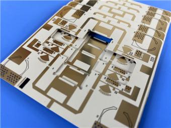
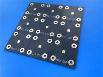
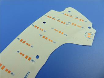
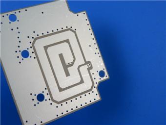
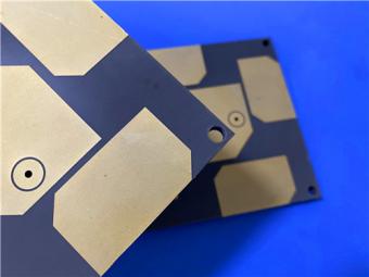
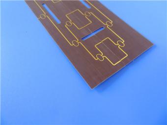
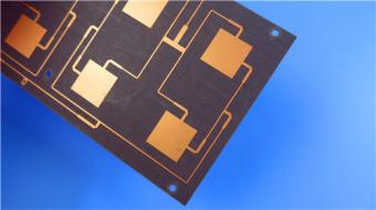
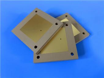
The TP440 PCB 59mil Immersion Gold Finish represents a purpose-built high-frequency circuit solution that leverages the exceptional dielectric properties of the Wangling TP440 thermoplastic substrate.
High-Frequency 2-Layer PCB on 59mil Wangling TP440 Thermoplastic Dielectric Immersion Gold
This article provides a comprehensive technical overview of the TP440 PCB, a 2-layer rigid high-frequency printed circuit board manufactured on a Wangling TP440 thermoplastic dielectric substrate with a 59mil (1.5 mm) core thickness and immersion gold surface finish. The document is organized into two distinct parts.
Part I details the PCB construction, layer stackup, and manufacturing statistics, highlighting the board's design parameters and quality standards.
Part II presents an in-depth examination of the TP440 copper-clad laminate (CCL) material, including its complete data sheet, material composition, electrical and thermomechanical properties, available specifications, and processing guidelines. Each part concludes with a dedicated summary to reinforce the key technical takeaways.
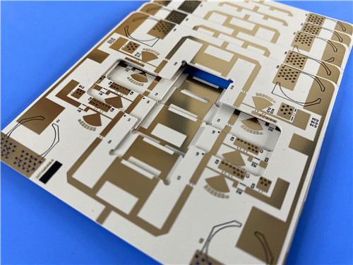
The Wangling TP440 PCB is a precision-engineered 2-layer rigid circuit board designed for high-frequency RF and antenna applications. Built on a 1.5 mm (59mil) TP440 dielectric core with 1 oz (35 μm) copper on both outer layers, the board achieves a finished thickness of 1.6 mm. The immersion gold surface finish provides excellent solderability, flat contact surfaces, and corrosion resistance — properties particularly valuable for RF connectors and high-frequency signal paths.
The following table summarizes the complete construction specifications of the TP440 high frequency PCB, covering dimensional tolerances, feature sizes, copper weights, surface finish, and quality control measures.
|
Parameter |
Specification |
|
Board Dimensions |
45.63 mm × 97.01 mm (1 PCS), ±0.15 mm |
|
Minimum Trace / Space |
5 mils / 8 mils |
|
Minimum Hole Size |
0.3 mm |
|
Blind Vias |
None |
|
Finished Board Thickness |
1.6 mm |
|
Finished Cu Weight (Outer Layers) |
1 oz (1.4 mils / 35 μm) |
|
Via Plating Thickness |
20 μm |
|
Surface Finish |
Immersion Gold |
|
Top Silkscreen |
Black |
|
Bottom Silkscreen |
None |
|
Top Solder Mask |
None |
|
Bottom Solder Mask |
None |
|
Electrical Test |
100% tested prior to shipment |
The stackup employs a symmetric 2-layer rigid structure with a thick TP440 dielectric core sandwiched between two 35 μm copper layers, providing a stable and predictable substrate for high-frequency signal transmission.
|
Layer |
Material |
Thickness |
|
Layer 1 (Top) |
Copper (ED Foil) |
35 μm (1 oz) |
|
Core |
TP440 Dielectric (PPO + Ceramic) |
1.5 mm (59 mil) |
|
Layer 2 (Bottom) |
Copper (ED Foil) |
35 μm (1 oz) |
The board accommodates 24 components across 19 pads with 28 through-hole vias, all organized under a single net — a configuration typical of dedicated antenna or RF feed structures.
|
Metric |
Count |
|
Components |
24 |
|
Total Pads |
19 |
|
Through-Hole Pads |
11 |
|
Top SMT Pads |
8 |
|
Bottom SMT Pads |
0 |
|
Vias |
28 |
|
Nets |
1 |
Several design choices distinguish this Wangling TPPCB from conventional FR-4 boards and contribute to its suitability for high-frequency applications:
· TP440 High-Frequency Substrate: Unlike standard FR-4 (Dk ≈ 4.3–4.6, Df ≈ 0.02 at 1 GHz), the TP440 core delivers a tightly controlled dielectric constant of 4.4 ± 0.09 at 10 GHz and an ultra-low dissipation factor of 0.0010, minimizing insertion loss in microwave circuits.
· Bare-Copper (No Solder Mask) Configuration: The absence of solder mask on both layers eliminates the dielectric perturbation caused by mask materials (typically Dk ≈ 3.0–3.5), ensuring the designed impedance and radiation characteristics remain unaltered — a critical requirement for antenna and millimeter-wave designs.
· Immersion Gold Finish: Compared to HASL (hot air solder leveling), immersion gold provides a flat, coplanar surface essential for fine-pitch RF connectors and surface-mount microwave components. It also offers superior shelf life and avoids the thermal stress associated with HASL processes.
· 5/8 mil Trace/Space Capability: The fine-line capability enables compact routing of high-impedance transmission lines and closely spaced ground via arrays, supporting the miniaturization goals of modern antenna systems.
· IPC-Class-2 Compliance with 100% E-Test: Every board is electrically tested to verify continuity and isolation, ensuring reliable performance in mission-critical applications such as missile-borne electronics and fuze systems.
The TP440 59mil PCB is engineered for high-reliability, high-frequency environments. Its combination of low dielectric loss, wide operating temperature range (-100 °C to +150 °C), radiation resistance, and low outgassing makes it particularly well-suited for the following applications:
· GPS and Beidou satellite navigation antennas
· Missile-borne RF electronics and guidance systems
· Fuze and proximity sensor circuits
· Miniaturized patch and waveguide antennas
· High-frequency RF transmission lines and power dividers
· Aerospace and defense communication subsystems
The TP440 PCB 59mil Immersion Gold Finish represents a purpose-built high-frequency circuit solution that leverages the exceptional dielectric properties of the Wangling TP440 thermoplastic substrate. With its symmetric 2-layer stackup, 1 oz copper construction, bare-copper (solder-mask-free) configuration, and immersion gold surface finish, the board is optimized for impedance-controlled RF and antenna applications where signal integrity and dimensional precision are paramount.
For engineers seeking a high-performance, cost-effective alternative to ceramic substrates and conventional high-frequency laminates, this TP440 PCB delivers a compelling balance of electrical performance, mechanical robustness, and manufacturing accessibility.
Part II: TP440 Copper-Clad Laminate (CCL) Material Knowledge
The Wangling TP series is a unique family of high-frequency thermoplastic copper-clad laminates developed specifically for microwave and millimeter-wave applications. Unlike conventional fiberglass-reinforced epoxy or PTFE substrates, TP-series laminates employ a dielectric layer composed of ceramic fillers dispersed in a polyphenylene oxide (PPO) resin matrix, with no glass fiber reinforcement. This composition enables precise tuning of the dielectric constant by adjusting the ratio of ceramic to PPO resin, allowing Dk values to be selected anywhere within the range of 3.0 to 25.0.
The TP440 designation refers to the TP-series variant with a nominal dielectric constant of 4.4. The product nomenclature follows a clear convention: TP denotes the bare dielectric material without copper cladding; TP-1 indicates single-sided copper-clad laminate; and TP-2 denotes double-sided copper-clad laminate. The PCB described in Part I utilizes a TP-2 (double-sided copper) configuration with 1 oz ED copper foil.
The TP440 dielectric consists of a homogeneous blend of polyphenylene oxide (PPO) resin and ceramic particulate fillers. The absence of woven glass fiber reinforcement yields several distinct advantages: the dielectric properties are isotropic (uniform in all directions), eliminating the "weave effect" that causes impedance variations in glass-reinforced laminates; the material can be machined using conventional methods including drilling, turning, grinding, shearing, and etching; and the copper-to-dielectric adhesion is achieved through direct resin bonding rather than through a glass fiber interface, resulting in more reliable peel strength than vacuum-metallized ceramic substrates.
The laminate is supplied with electrodeposited (ED) copper foil in two standard thicknesses: 0.018 mm (0.5 oz) and 0.035 mm (1 oz). The material density is 1.89 g/cm³, and the thermal conductivity is 0.44 W/(m·K), providing moderate heat dissipation capability for low-to-medium power RF circuits.
The following table presents the complete technical data sheet for the TP440 material, covering electrical, mechanical, and thermal properties measured under standardized test conditions (IPC-TM-650 / GB/T 4722-2017 / GB/T 12636-1990).
|
Property |
Test Condition |
Unit |
TP440 Value |
|
Dielectric Constant (Dk) |
10 GHz, Z-direction |
— |
4.4 ± 0.09 |
|
Dk Tolerance |
— |
— |
±2% |
|
Dissipation Factor (Df) |
10 GHz |
— |
0.0010 |
|
TCDk (Temp. Coeff. of Dk) |
-55 °C to +150 °C |
PPM/°C |
-50 |
|
Peel Strength (Normal) |
1 oz copper, ambient |
N/mm |
> 0.6 |
|
Peel Strength (After Humidity) |
1 oz, after humidity cycling |
N/mm |
> 0.4 |
|
Volume Resistivity |
500 V DC, ambient |
MΩ·cm |
> 1 × 10⁹ |
|
Surface Resistance |
500 V DC, ambient |
MΩ |
> 1 × 10⁷ |
|
CTE (X / Y / Z) |
-55 °C to +150 °C |
PPM/°C |
60 / 60 / 70 |
|
Water Absorption |
20 ± 2 °C, 24 hours |
% |
≤ 0.01 |
|
Long-Term Operating Temp. |
High/low temperature chamber |
°C |
-100 to +150 |
|
Material Composition |
— |
— |
PPO + Ceramic + ED Cu Foil |
|
Density |
— |
g/cm³ |
1.89 |
|
Thermal Conductivity |
— |
W/(m·K) |
0.44 |
As a thermoplastic material, TP440 requires specific processing considerations that differ from thermoset FR-4 and high-frequency laminates. The following guidelines are essential for successful fabrication and assembly:
TP440 laminatesare available in a range of standard panel sizes and thicknesses, with custom configurations available upon request.
Standard Panel Sizes (tolerance: -2 mm):
150 × 150 mm | 160 × 160 mm | 200 × 200 mm | 170 × 240 mm
Available Thicknesses and Tolerances:
|
Thickness (mm) |
Tolerance (mm) |
Thickness (mm) |
Tolerance (mm) |
|
0.5 |
±0.04 |
3.0 |
±0.10 |
|
0.8 |
±0.05 |
4.0 |
±0.10 |
|
1.0 |
±0.05 |
5.0 |
±0.12 |
|
1.2 |
±0.05 |
6.0 |
±0.12 |
|
1.5 |
±0.06 |
7.0 |
±0.15 |
|
2.0 |
±0.075 |
8.0 |
±0.18 |
|
Hot Tags :
TP440 PCB
TP440 copper-clad laminate
Wangling TP440 PCB
TP440 high frequency PCB
Wangling TP PCB
TP440 59mil PCB
If you have questions or suggestions,please leave us a message,we will reply you as soon as we can! Categories
New Products
Related Products
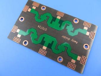
Polytetrafluoroethylene (Short for PTFE), commonly known as "plastic king ", is a polymer compound made of tetrafluoroethylene by polymerization. It has excellent chemical stability, corrosion resistance, sealing, high lubrication and non-viscosity, electrical insulation and good aging resistance. 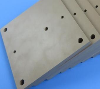
Rogers TMM4 thermoset microwave material is ceramic, hydrocarbon, thermoset polymer composite designed for high plated-through-hole reliability stripline and microstrip applications. 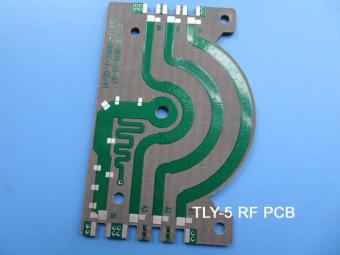
Taconic TLY laminates are a type of low loss laminates. They are manufactured with very light weight woven fiberglass and are more dimensionally stable than chopped fiber reinforced PTFE composites. 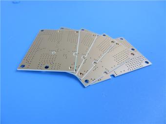
RO3203 laminates combine the surface smoothness of a non-woven PTFE laminate, for finer line etching tolerances, with the rigidity of a woven-glass PTFE laminate. These materials can be fabricated into printed circuit boards using 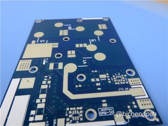
This type of immersion silver RF PCB is made on one of Taconic’s ORCER family material: RF-45. 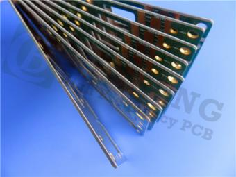
Rogers’ TMM10 thermoset microwave materials are ceramic, hydrocarbon, thermoset polymer composites designed for high plated-thru-hole reliability stripline and microstrip applications. 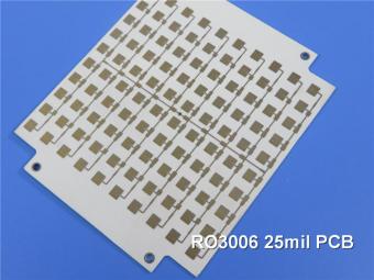
Rogers RO3006 was designed to offer exceptional electrical and mechanical stability at competitive prices. 
RT/duroid 6010LM microwave laminates feature ease of fabrication and stability in use. This property results in the possibility of mass production and reducing the cost of goods.


For inquiries about our products or pricelist, please leave to us and we will be in touch within 24 hours. © Copyright: 2026 Shenzhen Bicheng Electronics Technology Co., Ltd.. All Rights Reserved. 
IPv6 network supported
top
|