

 Call Us Now !
Tel : +86 755 27374946
Call Us Now !
Tel : +86 755 27374946
 Order Online Now !
Email : info@bichengpcb.com
Order Online Now !
Email : info@bichengpcb.com
Leveraging the advanced TFA 615 PCB substrate (Dk 6.15), this 2-layer PCB is engineered for high-frequency, mission-critical systems where performance, reliability, and environmental resilience are non-negotiable.
Item NO.:
BIC-397-v480.0Order(MOQ):
1-10Payment:
T/TProduct Origin:
ChinaShipping Port:
ShenzhenLead Time:
7-10 days
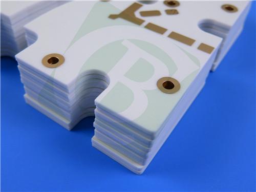
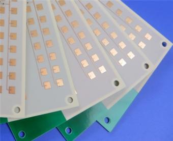
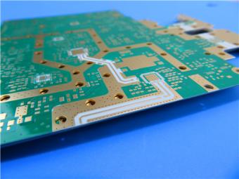
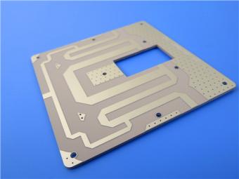
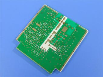
TFA615 PCB 2-layer 0.508mm 20mil Thick DK6.15 ENIG TFA Series Substrates
Introduction to TFA Series Substrates:
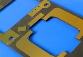
The TFA series PCB substrate represents a paradigm shift in dielectric substrate technology, built on a Polytetrafluoroethylene (PTFE) ceramic composite that abandons traditional manufacturing methods. Unlike conventional substrates produced by impregnating glass fiber cloth with resin, TFA substrates utilize an innovative process: prefabricated sheets are created through a proprietary technique and then pressed using a specialized lamination process. This breakthrough eliminates the limitations of glass fiber-based materials, positioning TFA as an aerospace-grade, high-frequency, and high-reliability alternative to comparable foreign products.
A key distinction of the TFA series PCB is the absence of glass fiber cloth. Instead, it incorporates a high concentration of uniformly dispersed special nano-ceramics blended with resin, which eliminates the "fiberglass effect"—a common source of electromagnetic wave propagation distortion in traditional PCBs. This results in exceptional frequency stability and minimal dielectric loss, outperforming materials in its class. Additionally, the TFA series minimizes X/Y/Z anisotropy, features a low thermal expansion coefficient (CTE) matching that of copper foil, and maintains stable dielectric properties across temperature fluctuations.
The TFA series offers four dielectric constant (Dk) options to suit diverse application needs:
2.94 (TFA294), 3.0 (TFA300), 6.15 (TFA615), and 10.2 (TFA1020).
Product Overview: TFA615 2-Layer 20mil PCB
Leveraging the advanced TFA 615 PCB substrate (Dk 6.15), this 2-layer PCB is engineered for high-frequency, mission-critical systems where performance, reliability, and environmental resilience are non-negotiable. It combines the material advantages of the TFA series with precision manufacturing to deliver a solution that excels in aerospace, defense, and satellite communication applications.

1. PCB Construction Details
The following table outlines the core construction specifications, each optimized to maximize the DK6.15 TFA PCB substrate’s performance and ensure compatibility with rigorous industry standards.
|
Specification |
Details |
|
Base Material |
TFA615 (PTFE ceramic composite substrate) |
|
Layer Count |
2 layers (rigid) |
|
Board Dimensions |
206mm x 54mm (1PCS) with ±0.15mm tolerance |
|
Minimum Trace/Space |
4 mils / 6 mils |
|
Minimum Hole Size |
0.3mm |
|
Blind Vias |
None |
|
Finished Board Thickness |
0.6mm |
|
Finished Copper Weight (Outer Layers) |
1oz (equivalent to 1.4 mils) |
|
Via Plating Thickness |
20 μm |
|
Surface Finish |
Immersion Gold |
|
Top Silkscreen |
No |
|
Bottom Silkscreen |
No |
|
Top Solder Mask |
No |
|
Bottom Solder Mask |
No |
|
Pre-Shipment Testing |
100% Electrical Test |
2.PCB Stackup
The 2-layer stackup is designed to complement the TFA615 substrate’s properties, ensuring efficient signal transmission and thermal management.
|
Layer Name |
Material/Component |
Thickness |
|
Copper Layer 1 |
Electrolytic Copper |
35 μm |
|
TFA615 Core |
PTFE Ceramic Composite |
0.508mm (20mil) |
|
Copper Layer 2 |
Electrolytic Copper |
35 μm |
3. PCB Statistics
These metrics reflect the PCB’s capability to support dense component integration, critical for high-frequency modules and rugged applications.
|
Category |
Quantity |
|
Total Components |
35 |
|
Total Pads |
153 |
|
Thru Hole Pads |
121 |
|
Top SMT Pads |
32 |
|
Bottom SMT Pads |
0 |
|
Vias |
77 |
|
Nets |
2 |
Key Features of TFA615 Substrate
Typical Applications
The TFA615 20 mil PCB is purpose-built for industries where performance and reliability are non-negotiable:
Quality & Availability
Conclusion
For engineers and buyers seeking a high-performance, cost-effective alternative to foreign aerospace-grade PCBs, the TFA615 2-Layer 20 mil PCB delivers unmatched value—combining technical excellence, global availability, and the durability to thrive in the world’s harshest environments.


Previous:
Wangling TP1020 PCB 2-Layer 4.0mm Thick ENIG TP Series High Frequency SubstratesNext:
Rogers RT/duroid 6202 PCB 2-layer 5mil 0.127mm ENIG Custom High Frequency BoardIf you have questions or suggestions,please leave us a message,we will reply you as soon as we can!
Categories
New Products
2-Layer 20mil FSD1020T ENIG High-Frequency PCB with Via Resin Plugged and Capped
4-Layer F4BM265+S1000-2M Material Hyrbid PCB with Blind Via Impedance Control & ENIG
4-Layer Wangling WL-CT338 + FR4 Hybrid PCB ENIG Green Solder Mask White Silkscreen
6-layer Isola 370HR High-Tg FR-4 PCB 2μ" ENIG Impedance Controlled
6-Layer RO4003C + FR4 Mixed Dielectric PCB with Hard Gold Plating Blind Via
30mil Taconic CER-10 2-layer Immersion Silver DK10 High Frequency Laminate PCB
31mil Rogers RT/duroid 5880 Double-sided Bare Copper ENIG Finished PCB
Wangling TFA294 Laminate 40mil Immersion Silver No Solder Mask Silkscreen Custom PCB

RF-10 25mil Taconic PCB Materials stands out as a high-performance solution for RF applications. Its exceptional electrical properties, dimensional stability, thermal conductivity, and adhesion characteristics make it an ideal choice for demanding applications.
The PCB has a 4-layer hybrid stackup with a 0.5oz+plating ground layer, two 1oz ground layers, and a 0.5oz+plating signal layer.
The dimensions of the board are 55.00 x 26.00 mm, with a tolerance of +/- 0.15mm. The board has 16 components, 26 total pads, 9 through-hole pads, 10 top SMT pads, 7 bottom SMT pads, 77 vias, and 82 nets.
Rogers RO4003C PCB is an innovative and advanced circuit board that is made with high-quality materials.
The RO4350B PCB offers a range of benefits that make it an ideal choice for high-frequency applications. Its low dielectric loss and high thermal conductivity make it perfect for high-frequency applications such as RF and microwave circuits.
Bicheng PCB Ships High-Quality PCBs with Shengyi Tg150 ℃ S1000H Material and Advanced Stackup
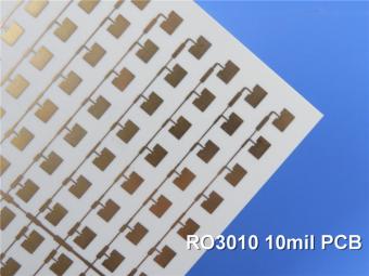
Rogers RO3010 PCB is ideal for a wide range of high-frequency applications, including power amplifiers, filters, couplers, and antennas.
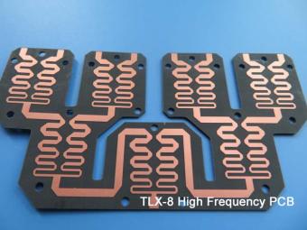
TLX-8 features low dielectric loss, low moisture absorption, and excellent thermal stability, making it ideal for high-frequency and high-speed applications. It has a low dissipation factor, which helps to minimize signal loss and distortion.
 6-11C Shidai Jingyuan, Fuyong, Baoan, Shenzhen, Guangdong, China 518103


For inquiries about our products or pricelist, please leave to us and we will be in touch within 24 hours.
© Copyright: 2026 Shenzhen Bicheng Electronics Technology Co., Ltd.. All Rights Reserved.

IPv6 network supported


