

 Call Us Now !
Tel : +86 755 27374946
Call Us Now !
Tel : +86 755 27374946
 Order Online Now !
Email : info@bichengpcb.com
Order Online Now !
Email : info@bichengpcb.com
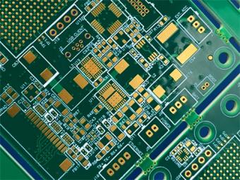
The TP1600 high frequency PCB integrates a high-performance TP1600 dielectric core with precision PCB engineering and pure gold surface finishing, creating an elite solution for high-frequency, high-reliability applications.
Item NO.:
BIC-565-v650.0Order(MOQ):
1-10Payment:
T/TProduct Origin:
ChinaShipping Port:
ShenzhenLead Time:
7-10 days
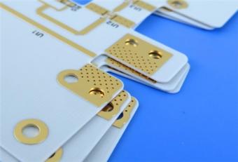
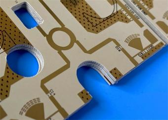
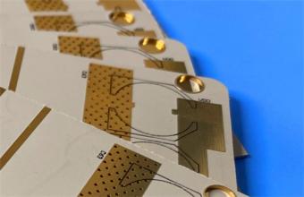
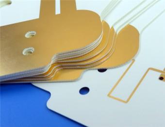
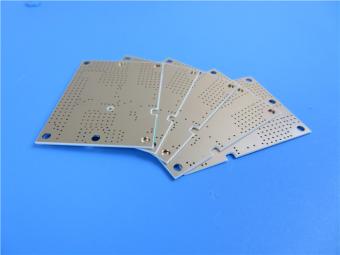
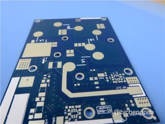
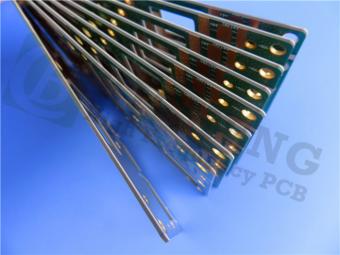
TP1600 PCB 31.49mil High DK16 Wangling Laminate Pure Gold Plating
1. Overview
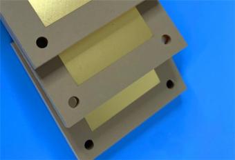
The TP1600 PCB 31.49mil Pure Gold Plating is a specialized 2-layer rigid high-frequency PCB built onTP1600 dielectric copper-clad laminate. Unlike standard FR-4 or high-frequency materials with glass cloth, Wangling TP1600 uses a ceramic-reinforced polyphenylene oxide (PPO) thermoplastic matrix without fiberglass, enabling precise dielectric control, uniform electrical performance, and freedom from weave effects that degrade microwave signal integrity. The pure gold plating surface finish ensures ultra-low contact resistance, stable impedance, corrosion resistance, and compatibility with precision assembly.
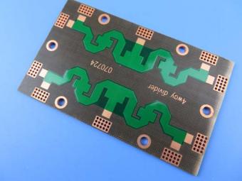
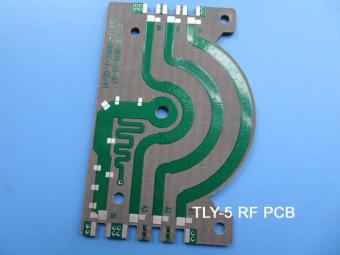
This Wangling TP PCB is optimized for miniaturized antennas, resonant structures, RF/microwave filters, couplers, high-frequency sensors, and aerospace systems including Beidou navigation, satellite payloads, missile-borne equipment, and fuzes. It combines high Dk, ultra-low dissipation factor, mechanical workability, and cost efficiency, making it a superior alternative to pure alumina or aluminum nitride ceramic substrates in many high-reliability scenarios.
2. PCB Construction
The following table summarizes the mechanical, electrical, and structural specifications of the finished PCB, defining its dimensional accuracy, line capability, plating, solder mask, silkscreen, and quality assurance parameters.
|
Item |
Specification |
|
Board Dimensions |
75 mm × 68 mm per piece, tolerance ±0.15 mm |
|
Minimum Trace / Space |
4 / 6 mils |
|
Minimum Finished Hole Size |
0.2 mm |
|
Blind Vias |
No |
|
Finished Board Thickness |
0.9 mm |
|
Finished Copper Weight (Outer Layers) |
1 oz (1.4 mils, ~35 μm) |
|
Via Plating Thickness |
20 μm |
|
Surface Finish |
Pure Gold Plating |
|
Top Silkscreen |
White |
|
Bottom Silkscreen |
White |
|
Top Solder Mask |
Green |
|
Bottom Solder Mask |
Green |
|
Electrical Test |
100% full electrical test before shipment |
3. PCB Stackup and Layer Structure
The PCB uses a symmetric 2-layer stackup centered on a 31.49mil TP1600 core, providing stable dielectric performance and balanced mechanical properties.
|
Layer |
Material |
Thickness |
|
Outer Copper Layer 1 |
Electrodeposited Copper |
35 μm |
|
Core Dielectric |
TP1600 High-Frequency Composite |
0.8 mm (31.49 mil) |
|
Outer Copper Layer 2 |
Electrodeposited Copper |
35 μm |
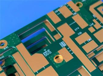
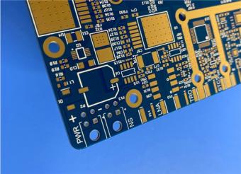
4. PCB Layout and Circuit Statistics
This table provides key circuit density and interconnection statistics, reflecting the compact, high-efficiency design suitable for miniaturized RF modules.
|
Parameter |
Quantity |
|
Mounted Components |
34 |
|
Total Pads |
56 |
|
Through-Hole Pads |
29 |
|
Top SMT Pads |
27 |
|
Bottom SMT Pads |
0 |
|
Vias |
34 |
|
Electrical Nets |
2 |

5. Core Advantages and Differentiators
5.1 Ultra-Stable High Dielectric Constant
TP1600 PCB substrate provides a nominal dielectric constant Dk = 16.0±0.32, tightly controlled via ceramic-to-PPO ratio adjustment. This enables significant circuit miniaturization while maintaining resonant performance ideal for compact antennas and resonant cavities.
5.2 Ultra-Low Dissipation Factor
With Df≈0.0012 at microwave frequencies, the material minimizes insertion loss and improves efficiency up to 10 GHz with little variation across frequency. This outperforms many general-purpose high-frequency substrates and approaches ceramic performance at lower cost.
5.3 No Glass Weave Effect
The absence of fiberglass cloth delivers a smooth, uniform dielectric layer, eliminating spatial Dk variation and signal scattering common in glass-reinforced materials. This is critical for high-yield, repeatable microwave performance.
5.4 Pure Gold Plating for High-Frequency Reliability
5.5 Excellent Mechanical and Thermal Stability
5.6 Process and Cost Advantages
Thermoplastic processability delivers higher yield and lower cost than alumina/AlN substrates. The Wangling PCB supports standard subtractive etching while avoiding the complexity of ceramic machining.
6. Recommended Assembly and Usage Constraints
To preserve performance and reliability, strict assembly rules apply:
7. Typical Target Applications
Appendix: Educational & Technical Reference–TP1600 Copper-Clad Laminate (CCL)
This section provides detailed material science and engineering data forTP1600PCB laminate, fully separated from the PCB description to avoid repetition.
1. Material Introduction
TP1600 is a specialized high-frequency microwave composite dielectric copper-clad laminate designed for compact, low-loss, high-stability RF/microwave circuits. It uses a ceramic-filled polyphenylene oxide (PPO) thermoplastic matrix without fiberglass reinforcement, manufactured via compression molding. The number“1600”denotes its nominal dielectric constant Dk = 16.0.
Key characteristics:

2. Full Datasheet Parameters of TP1600 CCL
*Note: All data are typical values based on standard test methods (GB/T 12636-1990, IPC-TM-650) and are provided for material selection guidance.*
|
Parameter |
Test Condition / Method |
Unit |
TP1600 Value |
|
Dielectric Constant (Dk, εr) |
5 GHz (Stripline, Z-axis) |
- |
16.0 ± 0.4 (Typical ±2.5%) |
|
Dissipation Factor (Df, tanδ) |
5 GHz |
- |
0.0015 |
|
Dk Temperature Coefficient (TcDk) |
-55°C to +150°C |
ppm/°C |
-40 |
|
Peel Strength (ED Cu, 1oz) |
Normal condition |
N/mm |
>0.6 |
|
After humidity/temp cycle |
N/mm |
>0.4 |
|
|
Volume Resistivity |
Normal, 500V |
MΩ·cm |
>1 x 10⁹ |
|
Surface Resistance |
Normal, 500V |
MΩ |
>1 x 10⁷ |
|
CTE (X / Y / Z - axis) |
-55°C to +150°C |
ppm/°C |
40 / 40 / 50 |
|
Water Absorption |
20±2°C, 24 hours |
% |
≤0.01 |
|
Density |
-- |
g/cm³ |
2.76 |
|
Thermal Conductivity |
-- |
W/(m·K) |
0.8 |
|
Long-term Operating Temperature |
Continuous |
°C |
-100 to +150 |
|
Copper Foil Type |
Standard |
- |
ED Copper |
|
Available Copper Thickness |
-- |
mm |
0.018 (0.5oz) , 0.035 (1oz) |
|
Material Composition |
-- |
- |
PPO + Ceramic, no glass fibers |
Copper Foil & Board Dimensions
|
Item |
Specification |
|
Copper Foil Type |
ED Copper Foil |
|
Copper Foil Thickness |
0.018 mm, 0.035 mm |
|
Available Panel Sizes |
150×150 mm, 160×160 mm, 200×200 mm, 170×240 mm |
|
Dimension Tolerance |
-2 mm |
Standard Thickness & Tolerance
Note: Thickness can be provided as total thickness including copper or dielectric thickness only. Please specify when placing an order. Non-standard thicknesses are available upon request.
|
Thickness (mm) |
0.8 |
1 |
1.2 |
1.5 |
2 |
3 |
|
|
Tolerance (mm) |
±0.05 |
±0.05 |
±0.05 |
±0.06 |
±0.075 |
±0.1 |
|
|
|
|
|
|
|
|
|
|
|
Thickness (mm) |
4 |
5 |
6 |
7 |
8 |
10 |
12 |
|
Tolerance (mm) |
±0.1 |
±0.12 |
±0.12 |
±0.15 |
±0.18 |
±0.2 |
±0.3 |
3. Material Structure and Performance Advantages
3.1 Dielectric Performance
3.2 Physical and Mechanical Traits
3.3 Thermal and Environmental Resistance
3.4 Manufacturing and Cost
4. TP1600 CCL Typical Application Fields
5. Why TP1600 Stands Out vs. Traditional Substrates
vs. FR-4: Much higher Dk, far lower Df, stable over temperature/frequency
vs. PTFE composites: Better dimensional stability, stronger copper adhesion, easier machining
vs. alumina/AlN ceramics: Lower cost, higher yield, drillable/processable with standard PCB equipment
vs. fiberglass-reinforced laminates: No weave effect, smoother surface, better impedance control
Conclusion
The TP1600 high frequency PCB integrates a high-performance TP1600 dielectric core with precision PCB engineering and pure gold surface finishing, creating an elite solution for high-frequency, high-reliability applications. It achieves a rare balance of ultra-high Dk, ultra-low loss, mechanical robustness, manufacturability, and cost efficiency, filling a unique niche between general PCBs and expensive ceramic substrates.
Backed by IPC-Class-2 quality, 100% electrical testing, and well-characterized TP1600 CCL performance, thishigh DK materialPCB ensures stable, repeatable, and reliable operation in aerospace, defense, satellite, and high-frequency sensor systems. Its pure gold finish, zero glass-weave distortion, and tightly controlled dielectric properties make it the preferred choice for mission-critical miniaturized microwave circuits requiring long-term stability and consistent electrical performance.


Previous:
WL-CT440 PCB 30mil 0.762mm Wangling Laminate ENIG Finish No Solder MaskNext:
TP2000 PCB TP Series 6mm Wangling DK20 Substrate Pure Gold Bare CopperIf you have questions or suggestions,please leave us a message,we will reply you as soon as we can!
Categories
New Products
RO4835 20mil Rogers Laminate 2-layer Immersion Gold Custom PCB
Rogers 20mil DiClad 527 PCB 2-layer Immersion Gold No Solder Mask Black Silkscreen
Wangling WL-CT300 5mil Laminate Pure Gold Plating High Frequency PCB
Wangling TF300 25mil DK3.0 Laminate 2-layer PCB Immersion Gold Black Silkscreen
2-Layer 0.5mm TP440 PCB Wangling TP DK4.4 Laminate Immersion Gold
20-Layer Panasonic TU872 HDI PCB ENEPIG 3.0mm Finished Thick Laser-drilled Blind Vias
10-Layer Rogers RO4003C + 370HR FR4 Hybrid Laminate PCB ENIG Impedance Control
8-Layer 10oz Heavy Copper TU-865 Substrate PCB With ENIG Blind &Buried Via
Polytetrafluoroethylene (Short for PTFE), commonly known as "plastic king ", is a polymer compound made of tetrafluoroethylene by polymerization. It has excellent chemical stability, corrosion resistance, sealing, high lubrication and non-viscosity, electrical insulation and good aging resistance.
Rogers TMM4 thermoset microwave material is ceramic, hydrocarbon, thermoset polymer composite designed for high plated-through-hole reliability stripline and microstrip applications.
Taconic TLY laminates are a type of low loss laminates. They are manufactured with very light weight woven fiberglass and are more dimensionally stable than chopped fiber reinforced PTFE composites.
RO3203 laminates combine the surface smoothness of a non-woven PTFE laminate, for finer line etching tolerances, with the rigidity of a woven-glass PTFE laminate. These materials can be fabricated into printed circuit boards using
This type of immersion silver RF PCB is made on one of Taconic’s ORCER family material: RF-45.
Rogers’ TMM10 thermoset microwave materials are ceramic, hydrocarbon, thermoset polymer composites designed for high plated-thru-hole reliability stripline and microstrip applications.
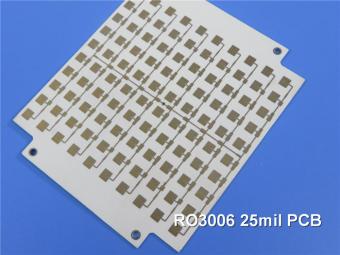
Rogers RO3006 was designed to offer exceptional electrical and mechanical stability at competitive prices.
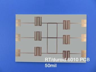
RT/duroid 6010LM microwave laminates feature ease of fabrication and stability in use. This property results in the possibility of mass production and reducing the cost of goods.
 6-11C Shidai Jingyuan, Fuyong, Baoan, Shenzhen, Guangdong, China 518103


For inquiries about our products or pricelist, please leave to us and we will be in touch within 24 hours.
© Copyright: 2026 Shenzhen Bicheng Electronics Technology Co., Ltd.. All Rights Reserved.

IPv6 network supported


