

 Call Us Now !
Tel : +86 755 27374946
Call Us Now !
Tel : +86 755 27374946
 Order Online Now !
Email : info@bichengpcb.com
Order Online Now !
Email : info@bichengpcb.com
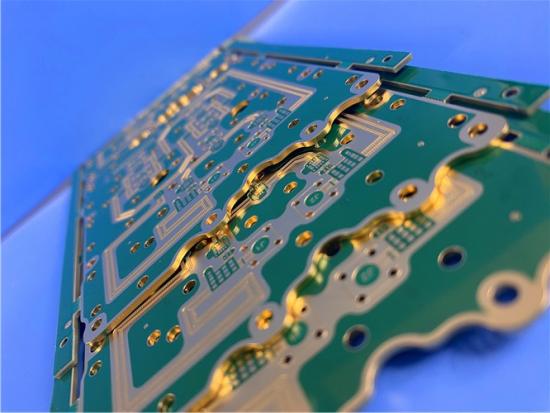
The 6-layer 10mil RO4350B + IT180A hybrid PCB represents a pragmatic engineering solution for high-frequency designs demanding both performance and cost consciousness.
Item NO.:
BIC-608-v693Order(MOQ):
1-10Payment:
T/TProduct Origin:
ChinaShipping Port:
ShenzhenLead Time:
7-10 days
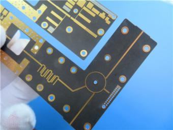
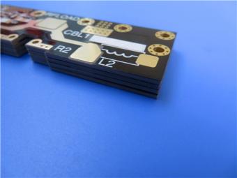
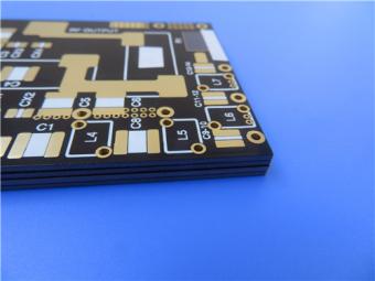
6-Layer 10mil RO4350B + IT180A Hybrid PCB with ENIG Blind Via Edge Plating
This6-layer hybrid PCB integrates Rogers RO4350B high-frequency laminates on the outer layer pairs with ITEQ IT-180A high-Tg FR-4 in the central core, delivering controlled-impedance RF performance on critical outer signal layers while maintaining cost efficiency and proven FR-4 processability for inner routing and power distribution. At 1.6 mm finished thickness with 10 mil (0.254 mm) RO4350B cores, the board targets applications from sub-GHz through millimeter-wave bands where low insertion loss, stable Dk over temperature, and reliable plated through-holes are essential. The hybrid architecture places low-loss dielectric precisely where RF signals travel, while the central FR-4 core provides structural rigidity and a cost-effective platform for digital and power-plane layers.
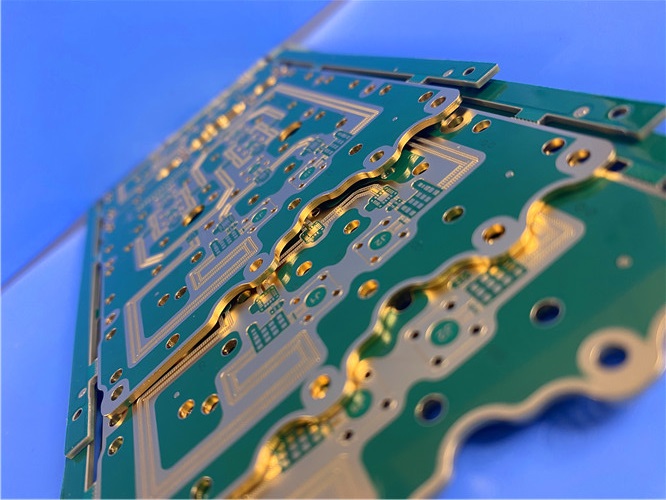
The table below summarizes the complete construction specifications of this hybrid PCB, covering base material, layer count, via architecture, copper weights, surface finish, and quality assurance measures.
|
Parameter |
Specification |
|
Base Material |
Hybrid — RO4350B (outer cores) + IT-180A (central core & prepreg) |
|
Layer Count |
6 layers |
|
Board Dimensions |
110 mm × 110 mm (1 PCS per panel) |
|
Blind Vias |
L1–L2, L3–L6 |
|
Finished Board Thickness |
1.6 mm |
|
Finished Copper Weight — Outer Layers |
1.42 oz (1 oz base + plating) |
|
Finished Copper Weight — Inner Layers |
1 oz (35 μm) |
|
Surface Finish |
Immersion Gold (ENIG) |
|
Top / Bottom Silkscreen |
White / White |
|
Top / Bottom Solder Mask |
Green / Green |
|
Edge Plating |
Yes |
|
Quality Assurance |
100% Electrical Test prior to shipment |
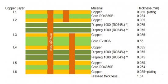
The layer stackup places RO4350B dielectric directly beneath the top and bottom signal layers, ensuring that high-frequency traces reference a low-loss, temperature-stable substrate, while the IT-180A central core provides structural rigidity and a stable platform for inner-layer power and ground planes. The total pressed thickness is 1.57 mm, reaching 1.6 mm after solder mask and plating.
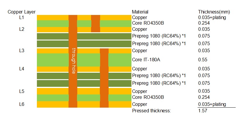
|
Layer |
Material |
Thickness (mm) |
|
L1 (Top) |
Copper (0.035 + plating) |
0.035 + plating |
|
|
Core RO4350B (10 mil) |
0.254 |
|
L2 |
Copper |
0.035 |
|
|
Prepreg 1080 (RC 64%) × 1 |
0.075 |
|
|
Prepreg 1080 (RC 64%) × 1 |
0.075 |
|
L3 |
Copper |
0.035 |
|
L4 |
Core IT-180A |
0.55 |
|
|
Copper |
0.035 |
|
|
Prepreg 1080 (RC 64%) × 1 |
0.075 |
|
|
Prepreg 1080 (RC 64%) × 1 |
0.075 |
|
L5 |
Copper |
0.035 |
|
|
Core RO4350B (10 mil) |
0.254 |
|
L6 (Bottom) |
Copper (0.035 + plating) |
0.035 + plating |
|
|
Pressed Thickness (Total) |
1.57 |
This RO4350B 6-layer hybrid PCB construction is well-suited for the following applications:
· Cellular base station antenna feed networks and power amplifiers
· Automotive radar (77 GHz) and ADAS sensor modules
· Satellite communication LNBs and phased array antennas
· RF identification (RFID) readers operating at UHF and microwave bands
· Test and measurement equipment requiring controlled-impedance multilayer routing
· Millimeter-wave sensors and 5G mmWave front-end modules
The 6-layer 10mil RO4350B + IT180A hybrid PCB represents a pragmatic engineering solution for high-frequency designs demanding both performance and cost consciousness. By placingRogers RO4350B low-loss dielectricprecisely where RF signals travel—on the outer layers—and using provenIT-180A high-Tg FR-4 for the structural core, the board achieves stable Dk over temperature, low insertion loss, and reliable multilayer fabrication without the premium of an all-high-frequency laminate. Combined with a blind-via architecture that minimizes signal stubs, ENIG surface finish for fine-pitch assembly, edge plating for EMI control, and 100% electrical test, this PCB delivers the signal integrity, reliability, and manufacturability required for demanding RF and microwave applications.
CCL Material Knowledge: Rogers RO4350B High-Frequency Copper Clad Laminate
Rogers RO4350B is a hydrocarbon ceramic-reinforced copper clad laminate (CCL) engineered specifically for high-frequency circuit applications from 500 MHz through millimeter-wave bands. Unlike PTFE-based microwave substrates, RO4350B is a rigid thermoset material that can be fabricated using standard FR-4 processing techniques, eliminating the need for specialized via preparation such as sodium etch. This manufacturability advantage, combined with its electrical performance and RoHS-compliant UL 94 V-0 flame retardancy, has made RO4350B one of the most widely adopted high-frequency laminates in the RF and microwave industry.
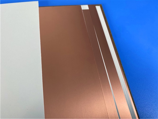
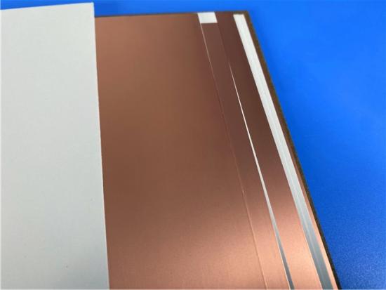
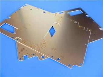
Figure 1. Rogers RO4350B copper clad laminate sheets with electrodeposited copper foil.
The following table presents the complete electrical, thermal, and mechanical properties of RO4350B as specified in the official Rogers datasheet (PUB# 92-004, Rev. 1592 080322).
|
Property |
Typical Value |
Direction |
Units |
Condition |
Test Method |
|
Dielectric Constant (εr) — Process |
3.48 ± 0.05 |
Z |
— |
10 GHz / 23 °C |
IPC-TM-650 2.5.5.5 |
|
Dielectric Constant (εr) — Design |
3.66 |
Z |
— |
8 to 40 GHz |
Differential Phase Length |
|
Dissipation Factor (tan δ) |
0.0037 / 0.0031 |
Z |
— |
10 GHz / 2.5 GHz, 23 °C |
IPC-TM-650 2.5.5.5 |
|
Thermal Coefficient of εr |
+50 |
Z |
ppm/°C |
−50 °C to 150 °C |
IPC-TM-650 2.5.5.5 |
|
Volume Resistivity |
1.2 × 10¹⁰ |
— |
MΩ·cm |
COND A |
IPC-TM-650 2.5.17.1 |
|
Surface Resistivity |
5.7 × 10⁹ |
— |
MΩ |
COND A |
IPC-TM-650 2.5.17.1 |
|
Electrical Strength |
31.2 (780) |
Z |
KV/mm (V/mil) |
0.51 mm (0.020") |
IPC-TM-650 2.5.6.2 |
|
Tensile Modulus |
16,767 (2,432) / 14,153 (2,053) |
X / Y |
MPa (ksi) |
RT |
ASTM D638 |
|
Tensile Strength |
203 (29.5) / 130 (18.9) |
X / Y |
MPa (ksi) |
RT |
ASTM D638 |
|
Flexural Strength |
255 (37) |
— |
MPa (kpsi) |
— |
IPC-TM-650 2.4.4 |
|
Dimensional Stability |
< 0.5 |
X, Y |
mm/m (mils/inch) |
After etch + E2/150 °C |
IPC-TM-650 2.4.39A |
|
CTE |
10 / 12 / 32 |
X / Y / Z |
ppm/°C |
−55 to 288 °C |
IPC-TM-650 2.4.41 |
|
Glass Transition Temp (Tg) |
> 280 |
— |
°C (TMA) |
— |
IPC-TM-650 2.4.24.3 |
|
Decomposition Temp (Td) |
390 |
— |
°C (TGA) |
— |
ASTM D3850 |
|
Thermal Conductivity |
0.69 |
— |
W/m/°K |
80 °C |
ASTM C518 |
|
Moisture Absorption |
0.06 |
— |
% |
48 hrs immersion, 50 °C |
ASTM D570 |
|
Density |
1.86 |
— |
g/cm³ |
23 °C |
ASTM D792 |
|
Copper Peel Strength |
0.88 (5.0) |
— |
N/mm (pli) |
After solder float, 1 oz ED |
IPC-TM-650 2.4.8 |
|
Flammability |
V-0 |
— |
— |
— |
UL 94 |
|
Lead-Free Process Compatible |
Yes |
— |
— |
— |
— |
Unlike PTFE-based laminates, RO4350B does not require sodium naphthalene etch or plasma treatment for via wall preparation before electroless copper deposition. It is fully compatible with standard FR-4 drilling, desmear, plating, etching, and lamination processes. The material is rigid enough for automated handling systems and scrubbing equipment, and it is lead-free process compatible with a UL 94 V-0 flammability rating using RoHS-compliant flame retardant technology. These characteristics mean that PCB fabricators can produce RO4350B-based boards on existing FR-4 lines without capital investment in specialized equipment, reducing both cost and lead time compared to PTFE-based alternatives.
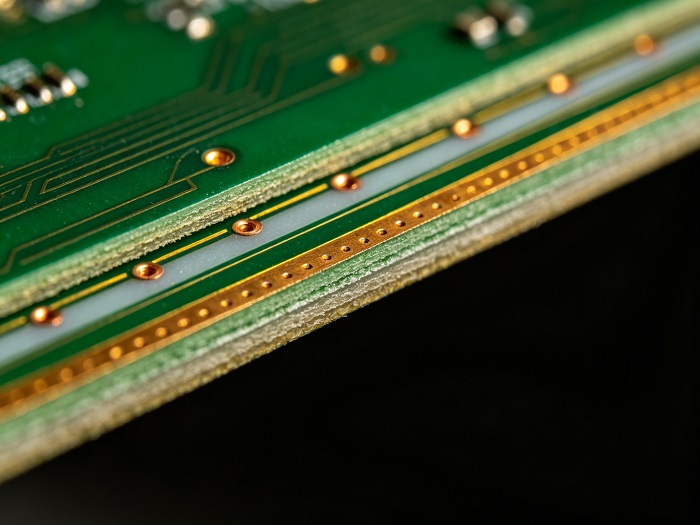
Figure 2. Cross-section of a high-frequency multilayer PCB showing layered dielectric and copper structure.
Rogers RO4350B occupies a unique position in the high-frequency CCL market: it delivers PTFE-level electrical stability and low loss while retaining the processability, mechanical robustness, and cost structure of an FR-4-compatible thermoset laminate.
Its process Dk of 3.48 ± 0.05, Df of 0.0037 at 10 GHz, TCDk of +50 ppm/°C, and Z-axis CTE of 32 ppm/°C collectively address the most critical requirements of RF and microwave circuit designers—stable impedance, low insertion loss, temperature resilience, and reliable plated through-holes. For the 6-layer hybrid PCB described in this document, RO4350B provides the high-frequency foundation on the outer layers, while its FR-4-compatible processing ensures seamless integration with the IT-180A central core in a single, manufacturable multilayer stackup. Designers seeking to push into higher frequency bands may further optimize conductor loss by specifying LoPro® foil, which reduces dielectric-side surface roughness by approximately 72% compared to standard electrodeposited copper.
Previous:
4-Layer 10mil RO3003 + Tg170 FR-4 Hybrid PCB with ENIG and Controlled Depth MillingNext:
4-layer 5mil RT6202 + FR-4 Hybrid PCB 1.014mm ENIG Resin Plug ViasIf you have questions or suggestions,please leave us a message,we will reply you as soon as we can!
Categories
New Products
Wangling F4BTMS220 2-Layer DK2.2 PCB 10 mil Core with Immersion Gold
Wangling F4BTME350 10mil DK3.5 High Frequency Substrate PCB 2-Layer Immersion Gold
Wangling F4BTM300 Custom 2-layer PCB 20mil DK3.0 Substrate with Immersion Gold
Rogers 20mil RT/duroid 6202 2-layer ENIG High-Frequency Microwave PCB
Rogers 20mil AD250C PCB Pure Gold High-Frequency Antenna Circuit Board
8-Layer Hybrid RF PCB: RO4350B + TG170 FR-4 + RO4003C with RO4450F Bondply
4-Layer Rogers RO3010 Hybrid PCB Immersion Silver 2.8mm Finished Thickness
4-Layer 20mil Rogers RO3210 ISIG High-Frequency PCB with Controlled Depth Milling
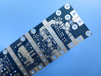
RO4003C exhibit a stable dielectric constant over a broad frequency range. This makes it an ideal substrate for broadband applications. And signal integrity performance improvement over the stack-ups with all FR4 board.
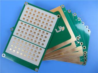
The hybrid PCB can be a mixture of FR-4 and high frequency material, and a mixture of high frequency material with different dielectric constant (DK)
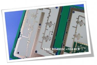
The 12mil core is on the top layer and it mainly plays the roles of signal layer. The core has fixed thickness which is very important to the electrical length of RF lines on the circuit board.
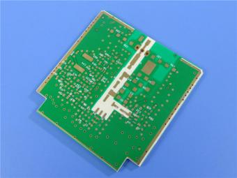
The hybrid PCB can be a mixture of FR-4 and high frequency material as abovementioned.
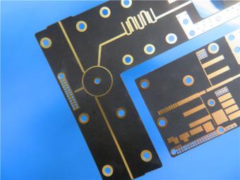
It contains 2 different boards in the panel. PCB boards are manufactured strictly as per required specifications with the standard IPC-Class-II.
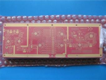
Hybrid PCB is also known as mixed material lamination, it’s normally combined by two different material like FR4 and PI(rigid flex PCB), FR4 and Ceramic, FR4 and Teflon, FR4 and Aluminum base etc.
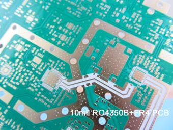
Hybrid constructions PCB typically involve a low loss material such as Nelco or Rogers combined with another core material like FR-4.
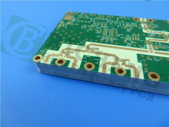
The Hybrid PCB on RO3003 and High Tg FR-4 is a state-of-the-art solution for high-frequency applications. With its exceptional stability, reliability, and manufacturability, it caters to the demands of industries such as automotive, telecommunications, and satellite communications.
 6-11C Shidai Jingyuan, Fuyong, Baoan, Shenzhen, Guangdong, China 518103


For inquiries about our products or pricelist, please leave to us and we will be in touch within 24 hours.
© Copyright: 2026 Shenzhen Bicheng Electronics Technology Co., Ltd.. All Rights Reserved.

IPv6 network supported


