

 Call Us Now !
Tel : +86 755 27374946
Call Us Now !
Tel : +86 755 27374946
 Order Online Now !
Email : info@bichengpcb.com
Order Online Now !
Email : info@bichengpcb.com
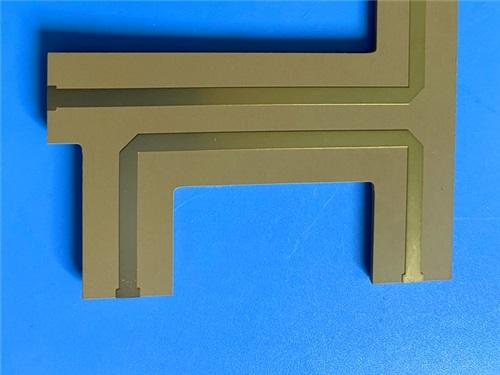
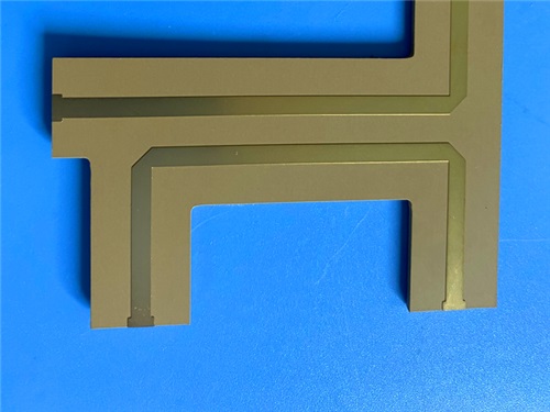
This article describes a two-layer rigid PCB built on Taizhou Wangling TF440, a woven-glass-free PTFE/ceramic composite on a 25 mil (0.635 mm) core with immersion gold.
Item NO.:
BIC-631-v716Order(MOQ):
1-10Payment:
T/TProduct Origin:
ChinaShipping Port:
ShenzhenLead Time:
7-10 days
Wangling TF440 25mil DK4.4 Laminate Immersion Gold 2-LayerCopper-filling Vias PCB
A Glass-Free PTFE/Ceramic Platform for Stable Microwave Circuits
This article describes a two-layer rigid PCB built on Taizhou Wangling TF440, a woven-glass-free PTFE/ceramic composite on a 25 mil (0.635 mm) core with immersion gold.
Part 1 covers construction, stackup, statistics, design choices and applications;
Part 2 explains theTF440 laminate with a complete data sheet, standard offerings and a CCL photograph. The combination targets microwave, antenna and RF front-end work needing stable dielectric constant, low loss and a wide temperature range.
1. The TF440 25 mil Immersion Gold PCB
1.1 Product overview
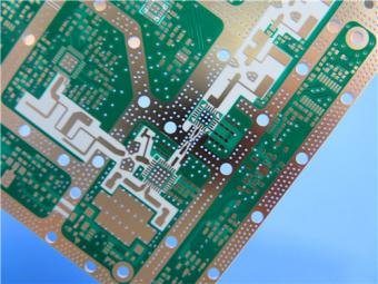
The TF440 25 mil immersion gold board is a double-sided, single-core RF panel, supplied as one 45 × 66.04 mm piece at ±0.15 mm tolerance. Both faces are clad with 1 oz (35 µm) copper on a 0.635 mm (25 mil) dielectric. It is built bare—no silkscreen or solder mask—so the controlled copper sits directly on the ceramic-filled PTFE.
The exposed copper is protected by immersion gold, with selected vias on a designated IC pad copper filled. Minimum trace/space is 7/8 mils, and the smallest drilled hole is 0.4 mm. The board is made to IPC Class 2 from Gerber RS-274-X artwork with 100% electrical test.
Table 1 lists the board’s key construction and finishing attributes.
|
Parameter |
Value |
|
Base material |
TF440 (PTFE + ceramic composite) |
|
Layer count |
2 layers |
|
Board dimensions |
45 × 66.04 mm = 1 PCS, ±0.15 mm |
|
Minimum trace / space |
7 / 8 mils |
|
Minimum hole size |
0.4 mm |
|
Finished board thickness |
0.7 mm |
|
Finished copper weight |
1 oz (35 µm), outer layers |
|
Via plating thickness |
20 µm |
|
Surface finish |
Immersion gold (ENIG) |
|
Top / bottom silkscreen |
No / No |
|
Top / bottom solder mask |
No / No |
|
Special construction |
Copper-filling vias on designated IC pad |
|
Quality / standard / artwork |
100% electrical test; IPC Class 2; Gerber RS-274-X |
Table 1. PCB construction details.
Table 2 shows equal 1 oz copper on both faces of the 25 mil core.
|
Layer |
Material / description |
Thickness |
|
Copper layer 1 (top) |
Electrodeposited copper, 1 oz |
35 µm |
|
Core |
TF440 dielectric (PTFE + ceramic, no glass) |
0.635 mm (25 mil) |
|
Copper layer 2 (bottom) |
Electrodeposited copper, 1 oz |
35 µm |
Table 2. PCB stackup (2-layer rigid).
Table 3 summarizes the pad, via and net counts.
|
Item |
Count |
|
Components |
60 |
|
Total pads |
45 |
|
Through-hole pads |
27 |
|
Top SMT pads |
18 |
|
Bottom SMT pads |
0 |
|
Vias |
26 |
|
Nets |
2 |
Table 3. PCB design statistics.
1.2 Engineering choices and differentiation
The bare-board configuration is the defining choice. On a microwave panel, a solder mask is itself a dielectric whose thickness, dielectric constant and coverage are poorly controlled. Leaving both faces without mask or silkscreen removes that variable from impedance and insertion-loss calculations, so every trace sees only the known 4.4 environment. The gold finish keeps the copper from oxidizing while preserving coplanarity for SMT and attach.
The copper-filling vias on the IC pad solve two problems at once: a filled and capped via gives the device a solid planar pad while creating a low-inductance path to the opposite face for grounding and RF return. With a single core and no lamination, faces stay in tight registration; the routing, holes and plating leave margin for IPC Class 2 yield.
1.3 Typical applications
With stable dielectric performance, low loss and a −80 to +200 °C service range, the board targets:
1.4 Conclusion (PCB)
The TF440 25mil PCB combines a symmetric single-core 2-layer build, 7/8 mil routing, 0.4 mm holes and a gold-finished, mask-free RF surface with copper-filled IC-pad vias. The result is a simple, reproducible, well-controlled platform for microwave and antenna work that values stable impedance and low parasitics over added layers or cosmetic coverings.
2. Understanding the Taizhou Wangling TF440 Laminate (CCL)
2.1 Material introduction
The board’s RF behavior is governed by its laminate. The Wangling TF series is a substrate made from PTFE resin, valued for its microwave properties, combined with ceramic fillers and no woven glass. Adjusting the ceramic-to-PTFE ratio controls the dielectric constant precisely, while a special process yields consistent performance and reliability.
The naming follows its cladding: TF is unclad, TF-1 single-sided clad and TF-2 double-sided clad. TF440 is the 4.4 grade, supplied here as double-sided clad with ED copper. The series offers dielectric constants from 3 to 16 with low dielectric loss.
2.2 Complete data sheet
Table 4 consolidates the complete published properties of TF440.
|
Property |
Test condition |
Units |
TF440 value |
Test method |
|
ELECTRICAL PROPERTIES |
||||
|
Dielectric constant (Dk) |
10 GHz, Z direction |
— |
4.4 ± 0.09 (≈ ±2%) |
Stripline, IPC-TM-650 2.5.5.5 |
|
Dissipation factor (Df) |
10 GHz |
— |
0.0010 |
IPC-TM-650 |
|
Temperature coefficient of Dk |
−55 to +150 °C |
ppm/°C |
−60 |
IPC-TM-650 |
|
Volume resistivity |
Normal, 500 V |
MΩ·cm |
>1×10⁹ |
IPC-TM-650 |
|
Surface resistance |
Normal, 500 V |
MΩ |
>1×10⁷ |
IPC-TM-650 |
|
THERMAL PROPERTIES |
||||
|
Long-term operating temperature |
Thermal cycling chamber |
°C |
−80 to +200 |
— |
|
Thermal conductivity |
Normal |
W/(m·K) |
0.32 |
— |
|
CTE, X / Y / Z |
−55 to +150 °C |
ppm/°C |
60 / 60 / 80 |
IPC-TM-650 |
|
MECHANICAL PROPERTIES |
||||
|
Peel strength (1 oz) |
Normal condition |
N/mm |
>0.6 |
IPC-TM-650 |
|
Peel strength (1 oz) |
After alternating damp heat |
N/mm |
>0.4 |
IPC-TM-650 |
|
PHYSICAL PROPERTIES |
||||
|
Density |
Normal |
g/cm³ |
2.58 |
— |
|
Water absorption |
20 ± 2 °C, 24 h |
% |
≤ 0.05 |
IPC-TM-650 |
Table 4. TF440 typical properties (complete data sheet).
Dk is measured in the Z direction by the stripline method (IPC-TM-650 2.5.5.5). Values are typical for selection, not a warranty; validate suitability for each application.
2.3 Standard offerings
Table 5 lists the standard foil, panel and thickness options.
|
Item |
Standard offering |
|
Copper foil |
ED foil; 0.018 mm (½ oz) or 0.035 mm (1 oz) |
|
Standard panel sizes |
150 × 150 mm; 250 × 250 mm (custom on request) |
|
Standard thicknesses (mm) |
0.635, 0.8, 1.0, 1.2, 1.5, 2.0, 2.5 |
|
Thickness tolerance (mm) |
±0.04, ±0.05, ±0.05, ±0.05, ±0.06, ±0.08, ±0.10 |
Table 5. TF series standard offerings.
Thickness may be total copper-clad or dielectric; specify which when ordering.
2.4 Technical analysis
The absence of woven glass is the key structural fact. Glass-reinforced laminates show a “glass-weave effect,” alternating between resin-rich and fiber-rich zones and causing periodic impedance variation and fiber-weave skew. TF440 instead disperses ceramic through a continuous PTFE matrix for a homogeneous dielectric, with ceramic loading fixing the nominal Dk. A Dk of 4.4 is a useful middle ground near FR-4, while its 0.0010 dissipation factor at 10 GHz sits in the low-loss PTFE regime rather than the several-thousandths of epoxy boards, reducing attenuation in feed lines.
The −60 ppm/°C TCDK describes a modest Dk drift, and water absorption ≤0.05% keeps properties stable in humidity. The grade supports continuous operation from −80 to +200 °C with radiation resistance and low outgassing for satellite hardware; density is 2.58 g/cm³ and thermal conductivity 0.32 W/(m·K). Chemical etching leaves its dielectric properties unchanged, and PTFE’s inert surface requires sodium-naphthalene or plasma activation for reliable hole metallization.
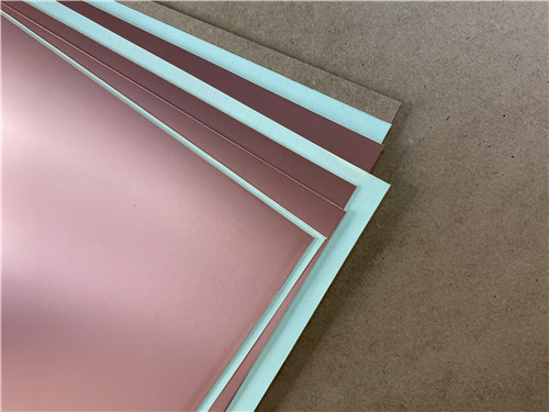
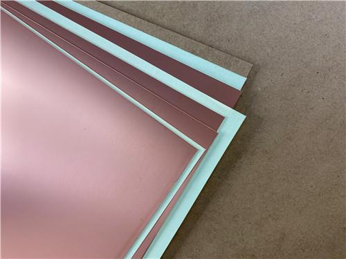
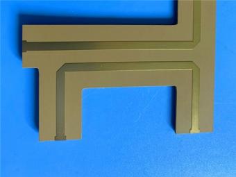
Figure 1. TaizhouWangling TF440 copper-clad PTFE/ceramic laminate sheets
Conclusion (CCL)
Wangling TF440 is a glass-free, ceramic-filled PTFE laminate pairing an FR-4-like 4.4 dielectric constant with PTFE-level low loss, very low water absorption, stable behavior and a −80 to +200 °C service range. Its homogeneous structure avoids the glass-weave effect, and its low-outgassing, radiation-resistant character suits microwave, antenna, satellite and aerospace RF circuits.
If you have questions or suggestions,please leave us a message,we will reply you as soon as we can!
Categories
New Products
Wangling TF440 25mil DK4.4 Laminate Immersion Gold 2-Layer Copper-filling Vias PCB
RO4360G2 Rogers 12mil ENEPIG 2-Layer DK6.15 High Frequency Custom PCB
Wangling F4BTMS220 2-Layer DK2.2 PCB 10 mil Core with Immersion Gold
Wangling F4BTME350 10mil DK3.5 High Frequency Substrate PCB 2-Layer Immersion Gold
Wangling F4BTM300 Custom 2-layer PCB 20mil DK3.0 Substrate with Immersion Gold
Rogers 20mil RT/duroid 6202 2-layer ENIG High-Frequency Microwave PCB
Rogers 20mil AD250C PCB Pure Gold High-Frequency Antenna Circuit Board
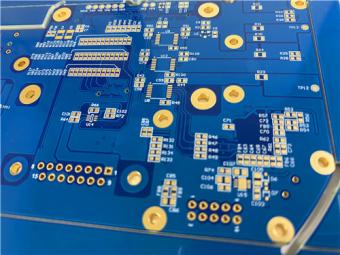
8-Layer Hybrid RF PCB: RO4350B + TG170 FR-4 + RO4003C with RO4450F Bondply
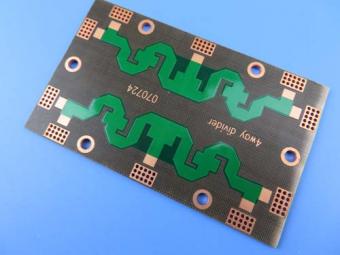
Polytetrafluoroethylene (Short for PTFE), commonly known as "plastic king ", is a polymer compound made of tetrafluoroethylene by polymerization. It has excellent chemical stability, corrosion resistance, sealing, high lubrication and non-viscosity, electrical insulation and good aging resistance.
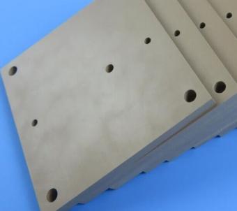
Rogers TMM4 thermoset microwave material is ceramic, hydrocarbon, thermoset polymer composite designed for high plated-through-hole reliability stripline and microstrip applications.
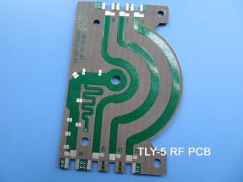
Taconic TLY laminates are a type of low loss laminates. They are manufactured with very light weight woven fiberglass and are more dimensionally stable than chopped fiber reinforced PTFE composites.
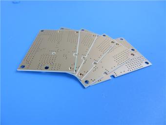
RO3203 laminates combine the surface smoothness of a non-woven PTFE laminate, for finer line etching tolerances, with the rigidity of a woven-glass PTFE laminate. These materials can be fabricated into printed circuit boards using
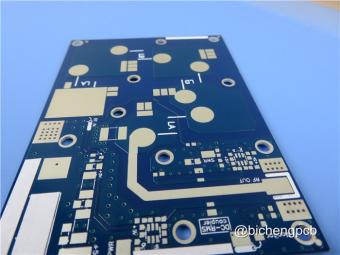
This type of immersion silver RF PCB is made on one of Taconic’s ORCER family material: RF-45.
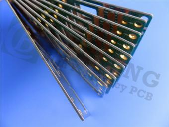
Rogers’ TMM10 thermoset microwave materials are ceramic, hydrocarbon, thermoset polymer composites designed for high plated-thru-hole reliability stripline and microstrip applications.
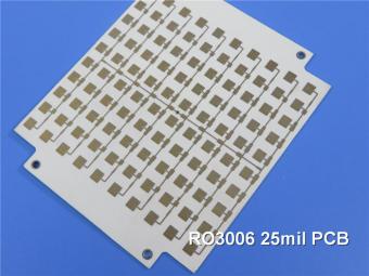
Rogers RO3006 was designed to offer exceptional electrical and mechanical stability at competitive prices.
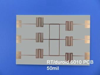
RT/duroid 6010LM microwave laminates feature ease of fabrication and stability in use. This property results in the possibility of mass production and reducing the cost of goods.
 6-11C Shidai Jingyuan, Fuyong, Baoan, Shenzhen, Guangdong, China 518103


For inquiries about our products or pricelist, please leave to us and we will be in touch within 24 hours.
© Copyright: 2026 Shenzhen Bicheng Electronics Technology Co., Ltd.. All Rights Reserved.

IPv6 network supported


